Hi Mooly,
You're right about using the proper test equipment as my old ears are far from being precise.
I do plan to play around more with these discrete devices before jumping on the OpAmp bandwagon. With that said, It's nice learn that OpAmps like the TL071/072 can function decently of a pair of batteries.
I've tried to follow some of the threads where you were helping people with some very sophisticated OpAmp power supplies and it just seemed overwhelming for a device that's supposed to have excellent PSRR and low power consumption.
Thanks again for all you help and suggestions!
You are welcome... gonna hit the off button now... some listening awaits 🙂
If you do play around with opamps, as long as you get the supplies the right way round, then they are pretty tough. Discrete, and it's easy to damage a transistor etc... but it's all part of the learning 🙂
Don't let those threads put you off, there we are aiming for perfection, and all that applies to wiring discrete circuitry too... opamps are simple and forgiving...
Enjoy and learn.
Hi
Regarding the circuit in post 16, the whole point of the follower is to lower the output impedance. I bet you could use a smaller resistor for R8 and run higher current say 20mA in the follower, and perhaps a larger output coupling cap. Or better....if you happen to have a J-fet of adequate conduction, you can replace R8 with a CCS, just connect the gate to the source of the fet. Then you have a singe end class A (small) power amp for the common emitter. Easy🙂
J-fet input stage does have it's advantages. If you get into audio electronics, you will acquire a love for J-fets.😉
BTW, if you notice on those small signal BJT's the current gain bandwidth decreases significantly when conducting less than 1 or 2 mA. You might try to re-bias the CE stage for at least couple of mA.
Hello CBS240,
Thank you for the suggestions. I'm open to any and all ideas.
While I don't have a bigger coupling capacitor handy, I will fiddle with some of the resistor values to try and boost the current flow above 2mA in both stages too see what happens.
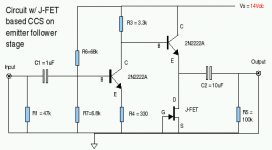
Also, I like your idea of applying a CSS to the emitter follower stage. While I don't feel a need to make this little preamp into a power amp, the CSS concept is intriguing to me as I suspect it might enhance linearity (and maybe PSRR as well). Please take a look at the attached sketch to see if I wired the J-FET properly.
Best regards,
Obe1
Thank you for the suggestions. I'm open to any and all ideas.
While I don't have a bigger coupling capacitor handy, I will fiddle with some of the resistor values to try and boost the current flow above 2mA in both stages too see what happens.
Also, I like your idea of applying a CSS to the emitter follower stage. While I don't feel a need to make this little preamp into a power amp, the CSS concept is intriguing to me as I suspect it might enhance linearity (and maybe PSRR as well). Please take a look at the attached sketch to see if I wired the J-FET properly.
Best regards,
Obe1
Attachments
Yep
The fet can be chosen based on Idss. It is good general practice to drive the input of the amplifier with lower impedance so that the input Z of the amplifier doesn't load down and effect the linearity of the pre-amp circuit. Just a buffer, which happens to be a power amplifer.🙂
The fet can be chosen based on Idss. It is good general practice to drive the input of the amplifier with lower impedance so that the input Z of the amplifier doesn't load down and effect the linearity of the pre-amp circuit. Just a buffer, which happens to be a power amplifer.🙂
That's a great idea of CBS240
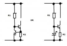
Something like a 2N3819 would be suitable... or you could use two npn transistors, or one npn and an LED.
In both cases R1 is chosen to provide enough bias current for the transistor. So around 4k7 would be a good starting point with a reasonably high gain transistor.
In the first example when the voltage across R2 reaches around 0.6 volts the lower transistor begins to conduct and this holds the current at a constant value by "shunting" away base drive from the pass transistor.
So the resistor value for say 10 ma would be
0.6/0.010 which is 60 ohms. So a 56 ohm would be ideal. By altering that value you get the current you require.
The second one uses an LED to provide a fixed voltage on the base. LED's make excellent low voltage references... different colour, different voltage 🙂 A red one will be around 1.8 volts. So 1.8 volts on the base gives an emmiter voltage of 1.8 - 0.6 which is 1.2 volts. That voltage is "constant" so you can now select a resistor (R2) to give your desired current. So 10 ma would be 1.2/0.010 = 120 ohms. R1 sets the "bias" and current through the LED as before so 4K7 again as a starting point.
The "open" collector would take the place of the drain of the FET.
Attachments
Last edited:
Hello Mooly, Thank you. This looks like fun. It's only 4:23 AM where I live, so my local parts store won't be open for another 6 hours. Rats! Thanks again!
Having LED Fun
Hi Mooley,
To better understand the various attributes of different biasing schemes, I went back to my original circuit (with collector to base biasing) as seen in Circuit 1A below. To my tin ears it produced the same level of gain as the circuit in Post #4 and sounded decent too.
While waiting for the parts store to open I found a red LED in my junk box and plugged it in place of resistor R4. Wow! Same volume out as before, yet the sound was noticeably more alive.
By my calculations, Circuit 1A should have a gain equal to about R3/R4 = 10K/1K = 10. In Circuit 1B, I assume the gain would be about R3/(voltage drop across LED/emitter current) = 10K/(1.7V/0.55ma) = 10K/3.1K = 3.22.
Interesting!?!?
Attachments

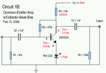
Keep in mind that in this circuit, R2 is providing some level of feedback. Av is not exactly the same as in a voltage divider bias circuit. (circuit in post #4)
R4 provides some degeneration to the transistor emitter, which is a form of feedback and results in a lowering of Hfe. Just one of the compromises you have to make in exchange for linearity.🙂 The diode has a fixed voltage, so gain becomes more a function of the device and Hfe, not the circuit parameters. In audio, at least IMO, it is better to design a circuit based on set circuit parameters and not so much on individual device variables.🙂 Others will disagree I'm sure.🙄
Anyway, learning being the objective, you should continue. If you ever get serious, a decent O-scope would be a good purchase.
The J-fet is so much simpler as a CCS in small signal situations because a depletion mode device, like a tube, will self bias and no other components are needed.😉
Hello CBS,
Thank you for following up. All of your points are all well taken. Please know CBS, that I have taken your advice about increasing the current flow in all of my circuits seriously (by whatever mechanism), yet regrettably some other (less fun) aspects of life have taken a higher priority today.
I really appreciate everyone's help and guidance in this forum. If all of you are not already employed as professional teachers, the formal institutions of education in this world could well benefit from your approach.
Most respectfully,
Obe1
Hi Obe,
Hmmm... well I'm not quite sure what that would sound like (your LED as shown). It will be very nonlinear... lots of harmonic distortion. It may produce a lot of "even harmonics"... the "good sort".
I've not made it clear enough what I meant with applying the CCS 🙂 sorry I assumed to much.
If you look at my two diagrams the constant current flows in the collector circuit (where the "break is) If you put a milliameter there, then with the values suggested you would find the current doesn't change as you alter the supply. It would be essentially the same at 5 volts or 15 volts or 50 volts.
So the CCS would be inserted in place of the JFET CBS240 suggested in post #23 as shown below.
I used this technique here (this is an all discrete germanium headphone amp).
http://www.diyaudio.com/forums/headphones/160646-germanium-single-ended-class-headphone-amp.html
Don't get confused by the "upside down" look and positive earth and PNP devices... just look how the transistors are configured... and the emmiter follower output Q3. The load for this follower is a CCS formed by Q4 and 5
Q2 and Q6 form a classic two transistor (NPN and PNP) gain stage that's non inverting of phase. You could try that in silicon.
Attachments

Hello Mooly,
Please know that your original instructions as to how the two CCS circuits worked, as well as where they should be applied in my circuitry was crystal clear. As I mentioned, you guys are great teachers.
Yesterday was a weird day that prevented me from getting out to acquire the components needed to experiment with the ideas you and CBS presented. When I found that red LED in my junk box, I remembered reading how some folks building vacuum tube amps used an LED in lieu of a traditional cathode resistor to set the grid bias on their triodes. This is what motivated me to try this on a transistor based amp. Nothing more that me being silly (again).
Take care!
Obe1
Hi Obe1... well it's great to experiment and to found out all these things for yourself.
And thanks for your kind words.
So what's the next project going to be ?
And thanks for your kind words.
So what's the next project going to be ?
Hey Mooly,
No new stuff right away. I think I owe to myself and my teachers to explore the ideas you've given me for my little BJT amplifier experiments. I've already tweaked some resistor values to the increase current flow (less the CCS goodies) just to see if I can judge what that does performance wise.
I must say though, that adding up all these ideas I'm going to run out of space on my breadboard very soon. Maybe dipping my toe into TL071 pool will have to come sooner than later. 😎
Best regards
If you are really interested I could try your circuit with the LED where you had it, and show what actually happens on the 'scope "for real" 🙂
Did you prefer the sound with it like that ?
Did you prefer the sound with it like that ?
Hello All,
I have a question regarding the polarity of coupling capacitors. I've studied a bunch of preamp schematics using both discrete components and integrated circuits. Some schematics show the input coupling cap in one direction and some have the polarity reversed. I Googled myself silly trying to understand this issue, but came up empty.
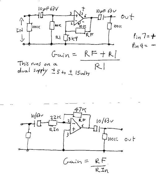
For example: Here's a link to a schematic of TL071 preamp that Mooly posted several years back on another thread with the input cap orientated minus to plus: TL071 circuit
And on this web page you can see another opamp schematic with the input cap orientated plus to minus: TL082 circuit
Best regards,
Obe1
I have a question regarding the polarity of coupling capacitors. I've studied a bunch of preamp schematics using both discrete components and integrated circuits. Some schematics show the input coupling cap in one direction and some have the polarity reversed. I Googled myself silly trying to understand this issue, but came up empty.
For example: Here's a link to a schematic of TL071 preamp that Mooly posted several years back on another thread with the input cap orientated minus to plus: TL071 circuit
And on this web page you can see another opamp schematic with the input cap orientated plus to minus: TL082 circuit
Best regards,
Obe1
Hello Mooly,
Thank you. That's very generous and I accept your offer. And yes, I did notice a marked difference in the sonics. I don't now all the flowery technical terms. All I can say is it sounded more alive.
Best regards & good listening,
Obe1
Thank you. That's very generous and I accept your offer. And yes, I did notice a marked difference in the sonics. I don't now all the flowery technical terms. All I can say is it sounded more alive.
Best regards & good listening,
Obe1
I vaguely remember drawing that...
As I draw them, the empty rectangle is the "positive end". The negative end should really be drawn as a black rectangle.
Now on a practical level, in the circuit in both links the voltage across the cap is actually zero (DC volts) so in a way it doesn't matter here.
If you used a TL071 on a "single" supply such as one 9 volt battery then the polarity is important of course.
With non FET opamps you do get a small "offset" voltage that could be either way, pos or neg, and although only a few millivolts it's worth actually measuring and orientating the caps to suit.
Your circuits as you draw them show the 1uf cap as a "non polarised" type like a film or polyester one. If you are using electroylitics for these then polarity is very important of course.
It's tea time 🙂
I'll hopefully rig your circuit up tomorrow.
It's tea time 🙂
I'll hopefully rig your circuit up tomorrow.
Hello Mooly,
Yes. The capacitors I'm currently using are a 1.0uF, non-polarized, film type.
Yes. If I were to replace these with electrolytic capacitors, I assume I would wire the minus side of the input cap to the base of the transistor and the plus side of the output cap to the collector of the transistor.
Thanks and I look forward to seeing your scope measurements.
Your circuits as you draw them show the 1uf cap as a "non polarised" type like a film or polyester one. If you are using electroylitics for these then polarity is very important of course.
Yes. The capacitors I'm currently using are a 1.0uF, non-polarized, film type.
Yes. If I were to replace these with electrolytic capacitors, I assume I would wire the minus side of the input cap to the base of the transistor and the plus side of the output cap to the collector of the transistor.
Thanks and I look forward to seeing your scope measurements.
Last edited:
- Status
- Not open for further replies.
- Home
- Source & Line
- Analog Line Level
- Basic Common Emitter Amp Help