KT,
Yes, years ago I learned to play piano and organ, but I was no Captain Nemo!!
I will dig up my textbook on acoustics and let you know.
Hugh
Yes, years ago I learned to play piano and organ, but I was no Captain Nemo!!
I will dig up my textbook on acoustics and let you know.
Hugh
Greg
I spotted your comment on your PCB about reversing other transistors that are used instead of the BD139/BD140.
Q3 using the 2SC1819 is no problem but I want to check what you have done with Q5 (2SC4793) and Q6 (2SA1837) when reversing these. From your pic at post #3 it looks like the middle amp has them standing up not contacting the heatsink and the right amp looks like they are bent to the heatsink touching on the front face. From your experience in running these, do Q5 and Q6 need to be on the heatsink or just left in air space? If they need to go on the heatsink I can cut the tracks and run some links.
I'm finally getting close to building now and have gone through all the hints / tips given and have decided the options / changes I am going to implement but leaving it as close as possible to the original schematic.
C1 = 1uF
LR (L=1.4uH) to be installed mid way between PCB and chassis
Zobel on board.... still deciding 10R or 2R7 resistor for R19???
Use 10R degeneration resistors from R3 to Q1 & Q2 (I think that's what Hugh meant in his post)
Use BP cap for C2
Q3 2SC1819
Q5 2SC4793
Q6 2SA1837
C5 = 47pF (because it's what I have and works with 2SC1819 on the AKSA)
Q1 and Q2 to be matched
100nF MKP suckout cap between TP3 and TP4
I was looking at adding a trimpot across R3 for DC offset control but never had issues on all the other AKSAs.... besides, I'd probably do it wrong.
I've restrained myself from using the real AKSA values and tricks as I want to see how this sounds with the hints /tips that have been discussed in this thread.
A few degrees warmer and I can get into it.
Cheers
Q3 using the 2SC1819 is no problem but I want to check what you have done with Q5 (2SC4793) and Q6 (2SA1837) when reversing these. From your pic at post #3 it looks like the middle amp has them standing up not contacting the heatsink and the right amp looks like they are bent to the heatsink touching on the front face. From your experience in running these, do Q5 and Q6 need to be on the heatsink or just left in air space? If they need to go on the heatsink I can cut the tracks and run some links.
Good eye. Yes when I did the first one I reversed Q5/Q6 and left them standing. There were a little close to the output spade, so on the next one I bend them forward out of the way. They aren't screwed down so there is no real contact with the heatsink. They run a few degrees warmer than the output transistors. My current feeling is they really don't need a heatsink, the original AKSA 55 didn't and I didn't have a problem over 5 years. As an option you could put the output spade under the PCB.
I'm finally getting close to building now and have gone through all the hints / tips given and have decided the options / changes I am going to implement but leaving it as close as possible to the original schematic.
C1 = 1uF
LR (L=1.4uH) to be installed mid way between PCB and chassis
Zobel on board.... still deciding 10R or 2R7 resistor for R19???
Use 10R degeneration resistors from R3 to Q1 & Q2 (I think that's what Hugh meant in his post)
Use BP cap for C2
Q3 2SC1819
Q5 2SC4793
Q6 2SA1837
C5 = 47pF (because it's what I have and works with 2SC1819 on the AKSA)
Q1 and Q2 to be matched
100nF MKP suckout cap between TP3 and TP4
I can't see your selections being a problem except for the degen resistors. I'm not an expert but I think you need to recalculate the LTP current if you add these.
I was looking at adding a trimpot across R3 for DC offset control but never had issues on all the other AKSAs.... besides, I'd probably do it wrong.
I have been amazed at the DC offset of this amp. The ones not using the BD139/BD140 (all 4) have very little offset, in the order of 3mV. This is the best I have ever had with any amp I have built.
BTW: I should mention, I expect there will be a need for more tuning of component values after some more testing.
regards
Last edited:
Thanks Greg.
I'll give the degeneration resistors a miss as I'm in no position to do the maths. So you are doing some fine tuning.... cool.
I'll give the degeneration resistors a miss as I'm in no position to do the maths. So you are doing some fine tuning.... cool.
Good eye. Yes when I did the first one I reversed Q5/Q6 and left them standing. There were a little close to the output spade, so on the next one I bend them forward out of the way. They aren't screwed down so there is no real contact with the heatsink. They run a few degrees warmer than the output transistors. My current feeling is they really don't need a heatsink, the original AKSA 55 didn't and I didn't have a problem over 5 years. As an option you could put the output spade under the PCB.
I can't see your selections being a problem except for the degen resistors. I'm not an expert but I think you need to recalculate the LTP current if you add these.
regards
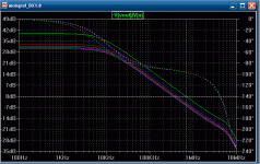
The degen resistors do not affect the LTP current , just the gain of the input pair (attachment 1). Plot shows 6 different degeneration R's {Rdgn), from 1R/20/40R etc. up to 100R.
Plot 2 shows how this affects the total loop gain of the amp with 42db at 1R and sub 30db @ 100R. What value you use is dependent on the beta of the input pair. My ksa/c's are best with 22r. MPSAxx or BCxxx are best with no resistors. Some zetex high gain pairs need 47R or more.
OS
Attachments
Rabbitz where are you sourcing the solid state components from?
I got them all from WES.
WES Components
I bought a dozen 2N5401 so they could be matched. IIRC, were less than $1ea so didn't break the bank.
It's alive today!
More of a AKSA 55N than a Baby AKSA as I didn't use the BD139/BD140 devices for the drivers and VAS. Only different by a few component changes, a couple of my own preferred component changes and a few additional components (most have been discussed in the thread) and headed that way since I used the drivers and VAS that's in the AKSA 55.
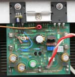
I used a 1uF input cap as have noticed a difference previously on speakers with a low F3. All electrolytics are Nichicon.... ES (C2), FG (C3, C10, C12), KZ (C4), KG (power supply). Q3 is 2SC1819, Q5 is 2SC4793, Q6 is 2SA1837 and all are reversed in the PCB due to opposite pin out to BD139/BD140. Silver mica for the phase lead and lag compensation caps. R3 was increased to reduce a larger than preferred -ve DC offset so it became < 10mV. The zobel is on the PCB and the output inductor // 10R 2W resistor are off board.
For the 1.4uH inductor I used 1.4mm wire x 10mm ID x 23 turns.
Alternative:
1mm wire x 10mm ID x 26 turns
1.4mm wire x 6mm ID x 32 turns
1mm wire x 6mm ID x 36 turns
There is a very gentle turn off thump and the amp runs luke warm. All voltages, bias etc came up trumps and more importantly, sounds like an AKSA right away. It has that special AKSA presentation, engagement and lively performance but retains smoothness. From experience, it will get better after 10-20 hours. It was run with a passive pre only and the performance surprised me as generally I have found AKSAs need a good active pre. The speakers used don't go that low (F3=60Hz) so probably helped the passive pre cause.
Thanks to Greg for the thread as well as supplying me his PCBs. I do have 2 of Greg's PCBs left over for anyone in Australia who wants them. Just send me a PM and I'll make it happen.
More of a AKSA 55N than a Baby AKSA as I didn't use the BD139/BD140 devices for the drivers and VAS. Only different by a few component changes, a couple of my own preferred component changes and a few additional components (most have been discussed in the thread) and headed that way since I used the drivers and VAS that's in the AKSA 55.
I used a 1uF input cap as have noticed a difference previously on speakers with a low F3. All electrolytics are Nichicon.... ES (C2), FG (C3, C10, C12), KZ (C4), KG (power supply). Q3 is 2SC1819, Q5 is 2SC4793, Q6 is 2SA1837 and all are reversed in the PCB due to opposite pin out to BD139/BD140. Silver mica for the phase lead and lag compensation caps. R3 was increased to reduce a larger than preferred -ve DC offset so it became < 10mV. The zobel is on the PCB and the output inductor // 10R 2W resistor are off board.
For the 1.4uH inductor I used 1.4mm wire x 10mm ID x 23 turns.
Alternative:
1mm wire x 10mm ID x 26 turns
1.4mm wire x 6mm ID x 32 turns
1mm wire x 6mm ID x 36 turns
There is a very gentle turn off thump and the amp runs luke warm. All voltages, bias etc came up trumps and more importantly, sounds like an AKSA right away. It has that special AKSA presentation, engagement and lively performance but retains smoothness. From experience, it will get better after 10-20 hours. It was run with a passive pre only and the performance surprised me as generally I have found AKSAs need a good active pre. The speakers used don't go that low (F3=60Hz) so probably helped the passive pre cause.
Thanks to Greg for the thread as well as supplying me his PCBs. I do have 2 of Greg's PCBs left over for anyone in Australia who wants them. Just send me a PM and I'll make it happen.
Attachments
I'm curious about the 2SD669/649. I can get them, along with 2SA1943/C1837, 2N5401/5551, and 2SA1943/C5200 for cheap at profusionplc.com, despite the higher shipping.
Can someone tell me the best source for silver mica caps in the US?
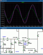
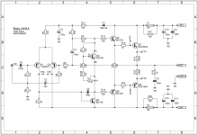
Schematic attached for reference.
- keantoken
Can someone tell me the best source for silver mica caps in the US?
Schematic attached for reference.
- keantoken
Attachments
There is a very gentle turn off thump and the amp runs luke warm. All voltages, bias etc came up trumps and more importantly, sounds like an AKSA right away. It has that special AKSA presentation, engagement and lively performance but retains smoothness. From experience, it will get better after 10-20 hours. It was run with a passive pre only and the performance surprised me as generally I have found AKSAs need a good active pre. The speakers used don't go that low (F3=60Hz) so probably helped the passive pre cause.
Thanks to Greg for the thread as well as supplying me his PCBs. I do have 2 of Greg's PCBs left over for anyone in Australia who wants them. Just send me a PM and I'll make it happen.
Hi rabbitz,
Thanks for posting your results. I hope you let us know more after the 10-20 hours breakin.
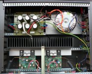
I like your solution to mounting the (reversed) drivers on the heatsink, simple but I didn't think of it. I notice you aren't a big fan of mounting components on the back of the PCB.🙂 These PCBs were designed for myself so I was experimenting with methods of reducing top PCB real estate. On the computer things always looked more cramped than in reality.
Any feedback on the PCB would be appreciated in case I decide to make a revision to the PCB in the future.
regards
Thanks, I will probably use them.
I really appreciate Greg's generosity.
Thanks Greg,
- keantoken
I really appreciate Greg's generosity.
Thanks Greg,
- keantoken
There is one concern I have for the design; offset is hard to trim, isn't it?
Even if the best values of R3 and R4 are picked, offset can vary. The BD139 is shown having near 100 Hfe, but a typical value is not specified implying that in practice it varies wildly. Current through the VAS is what, 8mA? So with a gain of 100 we'd have 80uA. 620mV across 2k makes 310uA, so in fact between an Hfe of 40 and 250, Q1 current can vary between 342uA and 510uA at DC (and this neglects Vbe differences), which becomes 0uA and 700uA if we assume a worst-case VAS output of +-8mA.
At DC this constitutes a 50% change in LTP balance, ouch. But we can change R3 to correct this, right? Anyways changing R4 will change VAS gain, using R3 is the most benign option it seems.
But wait, by the time we've corrected the imbalance, total LTP current is nearly twice it's original figure (remember the 50% balance change), and so the LTP's Gm is now halved, again we changed the circuit's characteristics.
Of course, in hindsight, correcting offset using R4 is better now because the decreased gain of the VAS will cancel with the increased gain of the LTP.
But still this isn't best because we still change the AC characteristics, by taking gain from the VAS and giving it to the LTP (and thus trade LTP distortion for VAS distortion).
This is a doomsday prediction of course. BD139's from the same batch might be reasonably matched, and if that is the case my preference would be to adjust offset using R4. Also consider the discussion on the effect of a balanced LTP on soundstage.
- keantoken
I have been amazed at the DC offset of this amp. The ones not using the BD139/BD140 (all 4) have very little offset, in the order of 3mV. This is the best I have ever had with any amp I have built.
Even the one using BD139/BD140 for VAS and drivers had reasonable DC offset, much less than 100mV.
Well if it's not a problem then, it's not a problem. But I was thinking it might be important if one wanted a balanced LTP.
- keantoken
- keantoken
KT,
Offset should be within +/-50mV on an audio amp.
On the AKSA, and the Baby AKSA, it's within 10mV plus and minus. This is more than sufficient since up to 500mV or so the majority of speakers don't much care about offset. Sure, it will displace the voice coil somewhat, and make excursion less linear in one direction than the other, but the dissipation of a 6.8 DCR voice coil at half a volt DC offset is only 37mW anyways, a walk in the park for a 35W continuous voice coil. Perfect balance and zero DC offset are elegant engineering notions, like pressure in the tire of an automobile, but in truth the speaker will work fine within quite wide extremes.
A balanced LTP is a wonderful idea and should be a design aim. But because of junction heating, there will always be a reduction of Vbe of around 2mV/degreeC at the VAS and this will change the balance situation (this assumes no current mirror, of course). If the VAS is TO126, dissipating less than 350mW, and is supplied with a heatsink, this drift will not generally be more than 30mV in practice. Thermal drift will cause reductions in linearity, no question, but the effect is slight, and most importantly, it is not discernible aurally. You can try very hard to pin the design down rigidily, but nature and the laws of physics will always find a way. But in this case, they do not affect the sound.
Cheers,
Hugh
Last edited:
Hi Greg
With over 8 hours on the amp it's a tad smoother but all else is the same. I don't think it will change much more.
The heatsink on the drivers seems to be cooler than the main heatsink (by touch) and that's only a little above room temperature. I'm sprung.... you caught me placing most items on the top of the PCB. I do it so I can spot any components getting hot or frying as well as I tend to bend components or leads under the PCB when handling during the build. There are only 4 components under the PCB.
I played with R3 again to reduce the offset to < 5mV. Even at it's worse was < 30mV at startup. The bias is rock solid with no drift. Each check was within 2mV of the set value.
Maybe some one can explain a DC offset circuit with a trimpot. I know there's a resistor and a trimpot but not sure of the configuration..... just in series so R3 has a wider range of say 30K to 60K? Are other components required?
Peter,
Obviously, in this form the amp is highly non-linear, but it's an essential parameter if we want to know the details of the feedback loop. You achieve this by putting an infinitely large cap (10,000uF in practice is normally enough) from the feedback node straight to ground, then put in a small, say 1mVp signal, and then measure the peak output of the amp loaded.
Hugh
Hello Hugh and all guys
Can this way, (putting an infinitely large cap from the feedback node straight to ground) to measure negative feedback factor, could work with an LTspice simulation ?
I have try it in few simulations but open loop numbers was way to high, especially with more complicated amps, so I may have missing something.
I can try it again, to experiment, using the Baby Aksa schematic or the asc file from anyone who have it, but I need to know the real life open loop gain and negative feedback factor (the feedback loop) to compared the sim results to the real life ones, anyone can tell me those ?
Thank you
Bye
Gaetan
Last edited:
- Home
- Amplifiers
- Solid State
- Based on Hugh Dean's AKSA 55