Hello
I have some extra THAD 1646 chip which even measure better than the DRV-134 .
You can look up the test on the net.
You can use as a replacement one by one to replace the DRV-134 chip.
The price for 1 chip $6.50
Greetings
I have some extra THAD 1646 chip which even measure better than the DRV-134 .
You can look up the test on the net.
You can use as a replacement one by one to replace the DRV-134 chip.
The price for 1 chip $6.50
Greetings
gaborbela said:Hello
I have some extra THAD 1646 chip which even measure better than the DRV-134 .
You can look up the test on the net.
You can use as a replacement one by one to replace the DRV-134 chip.
The price for 1 chip $6.50
Greetings
THAT 1646 not THAD 1646
MFR P/N 1646P08-U
Anthony
CJ900RR said:See this website. Both schematic shown there works like a charm!
http://sound.westhost.com/project14.htm
Improved versions have been posted at:
http://sound.westhost.com/project87.htm
TheSeekerr said:
No!
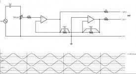
That is almost the same as the equivalent schematic as the DRV134 and will converts single-ended, ground-referenced input to a floating differential output with +6dB gain (G = 2).
Rod Elliotts schematic:
An externally hosted image should be here but it was not working when we last tested it.
DRV134 equivalent schematic:
An externally hosted image should be here but it was not working when we last tested it.
DRV134, SSM2142 and THAT1646 all converts single-ended, ground-referenced input to a floating differential output, witch is good when you have a balanced receiver in the other end. But to bridge two amplifiers you need a bridging adapter, such as Rod Elliotts project 14.
Hi CJ900RR,
While the schematic published on that page produces a floating output, the boards which can be purchased for P87b do not - this can be seen in the schematic on the secure section of his website, which I unfortunately cannot publish here.
While the schematic published on that page produces a floating output, the boards which can be purchased for P87b do not - this can be seen in the schematic on the secure section of his website, which I unfortunately cannot publish here.
Hi Seekerr.
Sorry I didn't know that, thank you for making that clear 🙂
I did read that he states that the boards for P87b can be used as a bridging adapter on the site for project 14, but I thought that people might misunderstood that the schematic on P87 is the same thing as P14.
But anyhow, the PCB's for P87B can be used as a bridging adapter, if you use the schematic in figure 2 shown at P14, or if you have access to the secure section of the site 🙂
bridging using balanced outputs
Question.
If the preamp is already fit with balanced output, could you bridge two standard gainclones (briangt's LM3886) directly??
Gerard
Question.
If the preamp is already fit with balanced output, could you bridge two standard gainclones (briangt's LM3886) directly??
Gerard
hi seems i still cant email folks o sorry for adding to this thread but,
Gaborbela: Do you by any chance have any of the THAD1646 chips left for sale? If so please email me.
many thanks
Nick
Gaborbela: Do you by any chance have any of the THAD1646 chips left for sale? If so please email me.
many thanks
Nick
CJ900RR said:See this website. Both schematic shown there works like a charm!
http://sound.westhost.com/project14.htm
I'm building the bpa300 amplifier, but i have problems with drv134 noise, so
i'm studying the possibility of bridging PA150 pcbs with ESP project 14. IT seems easy to do for me in a protoboard and point to point, but i have a doubt. Can i put a simple pot just before these circuit to avoid any preamplifier? What is the input impedance of this circuit?
Thanks
R1 & R4 set the input resistance.
Rin about 50k.
This can drive any sensible load impedance, >=2k
R5, R6 & R7 must be located very close to the output pins of the opamps. The TL series opamps do not like parasitic capacitance on the outputs.
Rin about 50k.
This can drive any sensible load impedance, >=2k
R5, R6 & R7 must be located very close to the output pins of the opamps. The TL series opamps do not like parasitic capacitance on the outputs.
Silicon Chip / Jaycar bridging kit / two way balanced line driver
Jaycar recently released a bridging kit:
http://jaycar.com.au/productView.asp?ID=KC5469
The PCB is a bit big as it shares with another project, but you can either cut it in half or buy the additional components and change to the other project:
http://jaycar.com.au/productView.asp?ID=KC5468
Which is a two way balanced line driver.
col.
CJ900RR said:Hi Seekerr.
Sorry I didn't know that, thank you for making that clear 🙂
I did read that he states that the boards for P87b can be used as a bridging adapter on the site for project 14, but I thought that people might misunderstood that the schematic on P87 is the same thing as P14.
But anyhow, the PCB's for P87B can be used as a bridging adapter, if you use the schematic in figure 2 shown at P14, or if you have access to the secure section of the site 🙂
AndrewT said:R1 & R4 set the input resistance.
Rin about 50k.
This can drive any sensible load impedance, >=2k
R5, R6 & R7 must be located very close to the output pins of the opamps. The TL series opamps do not like parasitic capacitance on the outputs.
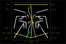
I go for this schematic. I'm now drawing the layout of the protoboard with one only quadruple opamp (TLE2074) for stereo configuration and SMD resistors 0,1% tolerance. The board will measure 40x40mm.
The 10uf input capacitor and the potentiometer will be out of the board.
The input capacitor will be this:
http://wduk.worldomain.net/acatalog...S_PXX_range.pdf
With this is not necesary a preamplifier.
Attachments
Hi J,
not all opamps like zero resistance in the unity gain feedback loop.
Some NEED a real resistance value between output pin and -IN pin.
Add a 1k resistor. It is still a unity gain non-inverting buffer.
Add some input filters.
Why the two 220pF caps on the inverting half channel?
That top 100r must be located very close to the left hand tl07x output pin.
AndrewT said:Hi J,
not all opamps like zero resistance in the unity gain feedback loop.
Some NEED a real resistance value between output pin and -IN pin.
Add a 1k resistor. It is still a unity gain non-inverting buffer.
Add some input filters.
Why the two 220pF caps on the inverting half channel?
That top 100r must be located very close to the left hand tl07x output pin.
i add the 1k resistor. The caps parallel to resistors are an advice of a friend to avoid noise, he said is to avoid any kind od gain at very high frequencies and also oscillations in the opamp.
About the input filters, a 2,2uf cap is enough. Is there any cap of this capacitance that i can use in a very small pcb. If not, i will use them out of the board, just after the pot.
Have you any preference about the quad opamp?
Thanks
is that decoupling connected to the signal ground?
9mV from a pair of FET input opamps seems a bit high.
I realise that FET input amps can tolerate much higher input resistance mismatches, but maybe your zero attempt to do any balancing of the input resistances of both opamps is resulting in this high offset.
Once you have a high offset it becomes much more susceptible to drift with temperature.
not dc offset, what i mean is 9mv ac signal in the output with the pot at the min.AndrewT said:is that decoupling connected to the signal ground?
9mV from a pair of FET input opamps seems a bit high.
I realise that FET input amps can tolerate much higher input resistance mismatches, but maybe your zero attempt to do any balancing of the input resistances of both opamps is resulting in this high offset.
Once you have a high offset it becomes much more susceptible to drift with temperature.
is this AC output a combination of noise and/or hum?juluska said:9mv ac signal in the output with the pot at the min.
Have you listened to it.
an ordinary speaker will reveal much about it.
A pair of headphones will reveal it at very loud level.
- Home
- Amplifiers
- Chip Amps
- Balanced line driver, PCB layout share