luka said:I gues trail and error is one way to see what will happen...
In the moment it seems to be the only way.
I am definitely struggling with something that you cannot see in the schematic. Without change in the schematic I can have shut downs at 15A or 35A, just depending on wiring... where from to reference which signal.... which path to use for high current... position of decoupling caps... etc... Unfortunately the observed behaviour does not always fit to my understanding of fields.. induced voltages... or typical parasitic effects.
...going a little blank in the moment...

Correction
...oohhhps, in posting #34 there is a mistake.
The power supply for the low side driver VCC must be pin 3, not pin 4 !
Come on... nobody noticed?
Anyway my suspects regarding inductive voltage drop on the wire between upper and lower MosFet seem to turn out more important than one would consider. You can easily find some ten volts voltage drop on that 50mm. ... also the voltage drop on the star point of neg supply is inconvinient... Wow, I have to rethink my design in several points, whereever high di/dt take place and from where to where I am referencing drive signals and measurement signals as well.
OK, class D in the kW range is becoming a cool playground.
...rookie learning steps...
10V on 5cm long wire?!?! As I remember that wire was pretty tick, for currents over 50A. That would have to have inductance of the motor...🙂
...if we assume that a wire is showing something like 5nH/cm (rule of thumb), then this wire had something like 25nH.... with di/dt around 1kA/us.... also calculation tells me 25V....
And as IRS20954 is sensing the Uds drop and driving upper MosFet with the same pin (VS)... you can chose:
- Poor current sensing (VS routing to drain of lower MosFet)
OR
- Poor gate drive (VS routing to source of upper MosFet)
Current sensing is more sensitive, so the second option is looking more reasonable... and reducing distance between MosFets...
I am seriously thinking about reducing the switching speed, but IRS20954S does not allow this. The Uds overcurrent sensing becomes active 200ns after the driver goes high. Means you must make sure, that the MosFet is really FULLY ON within 200ns. Naturally resulting in high di/dt.....
This background is limiting the suitability of IRS20954 to less high current applications.
... thinking about my IR2113 approach again.
ChocoHolic said:
- Poor current sensing (VS routing to drain of lower MosFet)
OR
- Poor gate drive (VS routing to source of upper MosFet)
Ohps ! Correction:
- Poor current sensing (VS routing to source of upper MosFet)
OR
- Poor gate drive (VS routing to drain of lower MosFet)
di/dt Hell
Aloha...
The more detailed I looked into this topic the more difficulties I discovered
In fact my high first results with something 30A..40A were just good luck and at that time I did not notice intermitting operation due to frequent shut downs. *lol*
OK... Summarizing my findings:
- Due to only 200ns blanking of the OC detection you must bring up the gate drive voltage up to about 10V within 200ns. This is determining the slowest allowed switching speed. And I found that with this the current commutation does take place in round about 20ns.
I cannot measure this at high currents due to several restrictions of my DIY equipment...
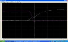
But you can see the necessary information also from the gate drive voltage. Current commutation at hard switching must take place in the time frame, after Ugs crosses the MOSFET treshold voltage and before the Miller plateau (neglecting the internal gate resistance of the MOSFET).
Red: Uds of lower MOSFET, 50V/grid , 1us/grid
White: Ugs of lower MOSFET, 5V/grid, 1us/grid
Aloha...
The more detailed I looked into this topic the more difficulties I discovered
In fact my high first results with something 30A..40A were just good luck and at that time I did not notice intermitting operation due to frequent shut downs. *lol*
OK... Summarizing my findings:
- Due to only 200ns blanking of the OC detection you must bring up the gate drive voltage up to about 10V within 200ns. This is determining the slowest allowed switching speed. And I found that with this the current commutation does take place in round about 20ns.
I cannot measure this at high currents due to several restrictions of my DIY equipment...
But you can see the necessary information also from the gate drive voltage. Current commutation at hard switching must take place in the time frame, after Ugs crosses the MOSFET treshold voltage and before the Miller plateau (neglecting the internal gate resistance of the MOSFET).
Red: Uds of lower MOSFET, 50V/grid , 1us/grid
White: Ugs of lower MOSFET, 5V/grid, 1us/grid
Attachments

...if we zoom into the details, we can see that the related times are short... hard to say exactly, may be about 20ns...
Means at 50A ==> di/dt = 2500A/us.
Means every nH causes a 2.5V voltage spike.
Means about 1V spike for each mm wire length.
Red: Uds of lower MOSFET, 50V/grid , 100ns/grid
White: Ugs of lower MOSFET, 5V/grid, 100ns/grid
Means at 50A ==> di/dt = 2500A/us.
Means every nH causes a 2.5V voltage spike.
Means about 1V spike for each mm wire length.
Red: Uds of lower MOSFET, 50V/grid , 100ns/grid
White: Ugs of lower MOSFET, 5V/grid, 100ns/grid
Attachments
That's tough.
And please note this is already the slow switching version....
Going on to summarize:
- I decided to slow down the switching by an additional cap between gate and source. This is preferable because it ensures low gate drive impedance and reduces the effect of the miller capacitance. You can realize reduced di/dt, but at the same time still fast dv/dt, which we like to have for 300kHz switching frequency. Also parasitic oscilations, which tend to take place with weak gate drive, are avoided.
- Handling the high di/dt requires some focus on the geometry. So I changed the meachnical position of my upper MosFet and directly connected its source pin to the drain plate of the lower MosFet. This helps to come down to some single nanoHenrys inbetween both MOSFETS.
- The wiring of VS and COM must be routed directly to drain and source of the lower MosFet, trying to sense the voltage mostly at the chip die inside....
- Perfect HF-blocking of the rails is mandatory. You need something like 5uF ...10uF with film caps directly from the drain of the upper MosFet to the source of the lower MosFet. The enclosed loop must be as small as possible!
- VSS should reference to the center tap of further film caps between the rails.
Have a look to the attached schematic, which might help to understand the above expalnations.
With all this, I am now able to handle really (no intermitting operation any more) something between 30A..40A also at hard switching. But not more.
My atempts with the IR2113 showed, that also this IC can be disturbed and furtheron it seems to be no good idea to run these MosFets at currents above 40A with hard switching and high frequency. It is possible to kill even these rugged devices.
So I am now planning to use seperate full bridges for each Sadhara cube. This keeps the currents in the range of 25A peak and allows 1kW for each cube (4 Ohms, Sadhara driver)...
Hi
With that cap on the gate of mosfet you create dead time or you reduce turn on speed of mosfet?
With that cap on the gate of mosfet you create dead time or you reduce turn on speed of mosfet?
Hi Luka,
the reason why I put this cap is to reduce di/dt, but of course it also influences the dead time and must be taken into consideration for dead time adjustment.
Fortunately dead time adjustment seems to be a simple topic. Let's say comparatively simple..
the reason why I put this cap is to reduce di/dt, but of course it also influences the dead time and must be taken into consideration for dead time adjustment.
Fortunately dead time adjustment seems to be a simple topic. Let's say comparatively simple..
I have never found any advantage associated with those 1uF to 10uF film caps that everybody seems to be placing across the supply rails near the output stage. The best that I have got out of them is ringing and more EMI due to higher dI/dt. I find a bank of plain low ESR high-ripple electrolytics far more convenient. LC filtering is obviously required if power supply wiring is involved.
Hi Eva,
that's strange! Seems like there are quite some unsolved topics in modeling/understanding what is really happening with such fast transients.
In fact in my set up, these film caps are quite helpful.
Without them I had some ringing of the halfbridge output voltage (refer to analogspiceman's thread, were I started with IRS20954). Regarding the undesired shut downs: A poor set up which was shutting down already at 15A improved be factor 2 just by placing these caps!
Thanks for your mail. I will also keep your RC-snubbering in mind for my next full bridge set up.
BTW: Your working times are making me afraid!!!!
Hi Eva,
that's strange! Seems like there are quite some unsolved topics in modeling/understanding what is really happening with such fast transients.
There is a lot of people doing things in a particular way just because they saw other people believed to be more wise doing the same, and very little people willing to investigate circuits in detail (just because they are already believed to work).
...yes, many people do not like to examine things in detail..
But from my experience, such behaviour usually leads to poor results, except somebody is just copying a bullet proof design.
Go to bed little lady!!! ...I will go to the gym now, even if this is sometimes boring. My back is thanking this by an unbelievable extend. It simply turned trouble free since I am doing some frequent exercises.


Eva said:😀😀😀
That's a nice aluminium plate, but be careful with weight gain 😉
Wasn't there a law of conservation of mass?

In fact the aluminium plate is just about 200g..., but gained 1.5kg during the last 3 days...
Hm, ... here some pics of my new output inductor...
A 6xEF25-scrap design.
Attachments
- Status
- Not open for further replies.
- Home
- Amplifiers
- Class D
- Babysteps of 1kW Class D Rookie Amp