BOM
...and for further information the BOM with some additional informations... Yes, I would also prefer to have this in the schematic, but then you always need to have the proper component name in the eagle libraries. 🙄
P.S:
Luka,
The PWM is generated by the comparator with hysteresis and positive feedback.
The input signal for this board is a normal analog audio signal, which may come from any OP amp (Should be a low impedance signal source and signal magnitude matched to the gain of Rookie. Gain of Rookie can be adjusted by R21, R31, R_NFB1, R_NFB2 ==> behaviour like a normal fully differential amp.)
Attachments
Hi
Checked the irs20954 datasheet.
It seems a good choice!
It looks to me that possibility of using "floating pwm input" makes it much easier to implement in class D design than popular IR20xx family.
What is your output inductor (core?) and switching frequency? You have very low HF signal at speaker.
Good work!!!
regards
Adam
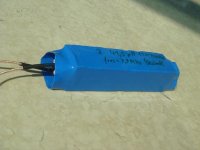
Currently I am working with slightly above 100kHz, but the switching behaviour and losses are pretty OK and so I am thinking about stepping up to 300...400kHz and enable the design for full audio bandwidth.
My current output choke is far from any optimized design.
I just quick & dirty used some excess ferrite scrap in my assortment. Means the core is a stacked 15xEF25 resulting in a huge Ae of 750mm^2 .
This geometry is unfortunately resulting in a quite unpleasant ratio of wire length per turns vs Ae and with this in unnecessary high Rdc and lowered resonance frequency compared to an optimzed design. Also overall size is large. ....but well using up what you have....
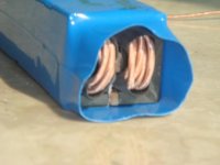
Instead of a bobbin I bundled the wires with an insulating sleeve inside the core.
The air gap is 2.2mm. Number of turns: 10
Wire: HF-Litz 150x0.1Culs.
I also examined solid wire, but the eddy current losses of the leaking field from the air gap heated up the choke about 10C already from +/- 3A/100kHz idle current in the filter. Now with this litz there is no self heating at idle situation at all.
Rdc is around 50m Ohms.
L is about 42uH.
Resonance frequency of the choke is 7.7MHz.
Saturation is theoretically somewhere around 60A (not measured up to now).
For optimization I am thinking about an ACP cut core which allows 3-4 times more flux density than ferrite and still offers reasonable HF-core-losses.
My current output choke is far from any optimized design.
I just quick & dirty used some excess ferrite scrap in my assortment. Means the core is a stacked 15xEF25 resulting in a huge Ae of 750mm^2 .
This geometry is unfortunately resulting in a quite unpleasant ratio of wire length per turns vs Ae and with this in unnecessary high Rdc and lowered resonance frequency compared to an optimzed design. Also overall size is large. ....but well using up what you have....
Instead of a bobbin I bundled the wires with an insulating sleeve inside the core.
The air gap is 2.2mm. Number of turns: 10
Wire: HF-Litz 150x0.1Culs.
I also examined solid wire, but the eddy current losses of the leaking field from the air gap heated up the choke about 10C already from +/- 3A/100kHz idle current in the filter. Now with this litz there is no self heating at idle situation at all.
Rdc is around 50m Ohms.
L is about 42uH.
Resonance frequency of the choke is 7.7MHz.
Saturation is theoretically somewhere around 60A (not measured up to now).
For optimization I am thinking about an ACP cut core which allows 3-4 times more flux density than ferrite and still offers reasonable HF-core-losses.
Attachments
ChocoHolic said:Currently I am working with slightly above 100kHz, but the switching behaviour and losses are pretty OK and so I am thinking about stepping up to 300...400kHz and enable the design for full audio bandwidth.
Switching frequencies as low as 200-250kHz will work fine for full audio bandwidth (i.e. up to 20kHz) and will probably allow your design to operate more efficiently. Very nice project by the way. Thank you for sharing with us 🙂
Hi ChocoHolic
For D8,D9 you said
For D8,D9 you said
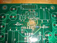
What do you mean here? Aren't GNDs connected together?GND connection of D8 is at Power GND, but should be clean signal GND. Reroute manually...
GNDs are connected together, you can see it in the picture of the PCB, GND side.
But you always have to take care with GND.
You must make sure that all signals are referencing to the same potential and if you run high currents through signal GND tracks then the GND potential is depending on the position were you connect to this GND track.
Any error signal on this track is adding to the audio signal and most accidential add ons do degrade the behaviour.
...it's just about controlling which paths do which currents take...
Simply assume that any copper track is series connection of many small R and L, with additional parasitic capacitances to any close track or component. ...so don't believe GND = GND...
Have a look to several threads regarding different GND routing philosophies.
... my laptop went dead this weekend.... 🙄
And without laptop I don't have a scope
So I first have to get it repaired ... delaying my class D amp again
Well, nevertheless some more infos from the last days.
I was pushing my proto to something like 320kHz and had to reduce the gate drive resistors to 5.6 Ohms ...uhhh now dv/dt in hard swithcing condition is around 5kV/us. Right at the specified limit of 5.5kV/us for my MOSFETs. Output filter choke was reduced to something around 10uH.
The triangular inductive ripple current of the output filter is really nice to provide perfect ZVS in idle condition. 😎
Also I had to strengthen the IC supply, driving two 150V/60A/32mOhm MOSFETs at 320kHz is demanding some current....
Furtheron I noticed that the required driver currents are depending on the MosFet load.
In ZVS condition, Uds has already reached zero, when turning on. So Ugs can be pulled up quite easy. Almost no Miller plateau. But if the output load is high and no ZVS anymore, but hard switching... Then Uds is ramping down due to turning ON process of the MosFet. The driver has to deliver the additional charge for the drain-gate capacity and must draw this from the IC supply.
Different from ZVS condition, during hard switching the Miller plateau is becoming quite strong. So already here you can see that the drivers have to deliver longer high currents to turn ON the MOSFETs.
In ZVS the charge for the drain-source-capacitance of course also has to be delivered, but then it is delivered from the load circuit and the MOSFET driver does only conduct it through the freewheeling diodes of the driver output or sink the charge to GND or VS respectively . Means this charge does not cause any stress
to the IC supply.
How does look in the overall current consumption of the IC, which has to deliver the current for upper and lower driver together? Let's give some names first. The freewheling diode in the high side driver from pin HO to pin VB is D_fw1. The freewheling diode in the high side driver from pin VS to pin HO is D_fw2.
The freewheling diode in the low side driver from pin LO to pin VCC is D_fw3. The freewheling diode in the low side driver from pin COM to pin LO is D_fw4.
Charge of the drain-gate-capacity of the upper halfbridge MOSFET is called Q_ds1.
Charge of the drain-gate-capacity of the lower half bridge MOSFET is called Q_ds2.
Situation a), ZVS:
Sloping upwards, Q_ds1 is delivered through D_fw2 and Q_ds2 is sinked by the low side driver towards GND.
Sloping downwards, Q_ds1 is sinked through the high side driver towards VS and Q_ds2 is delivered through D_fw4 to GND.
Situation b) high negative output current of the amp:
Upper switch is in ZVS, lower switch is hard switching.
Sloping upwards, Q_ds1 is delivered through D_fw2 and Q_ds2 is sinked by the low side driver towards GND.
Sloping downwards, Q_ds1 is sinked by the high side driver from VS and Q_ds2 has to be delivered by the low side driver out of VCC.
So we have to deliver per period one time Q_ds2, stressing the IC supply. ==> -1 Q, means some additional load for the IC supply.
Situation c) high positive output current of the amp:
Upper switch is hard switching, lower switch is in ZVS.
Sloping upwards, Q_ds1 has to be delivered by the high side driver out of VB and Q_ds2 is sinked by the low side driver from GND.
Sloping downwards, Q_ds1 is sinked by the high side driver from VS and Q_ds2 is delivered through D_fw4 towards GND.
So we have to deliver per period one time Q_ds1, stressing the IC supply. ==> Also -1 Q, means also some additional load for the IC supply.
Hm, in real life I am observing one additional effect.
Besides generally increased current consumption during hardswitching. I always see (also at no load and nice ZVS), that the IC is consuming more current during positive signal half waves compared to negative halfwaves. This might be related to IC internal structures, which might need more supply current for HIGH state and less supply current for LOW state.
And during the positive half waves we have longer times HIGH state and shorter times LOW state.
Sorry, no screen shots this time. All lost in my dead laptop... 😡
Interesting reading. Nice work.Your data may still be recovered if hard drive didn't fail and you don't wont to spend some additional money for that reason.If it didn't there is a way to get almost all if not all of data back or just the things you need most. Please do let me know.
Today, the CPU went into smoke on my Linux box containing all my cad and simulation files. Murphy really does his best to hinder the progress in class d 😉
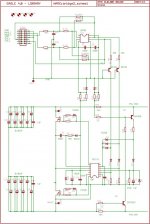
Intermediate 2113 Trials
I got annoyed and had the feeling that the IRS20954S would be oversensitive...
So I set up an trial design with the IR2113 according the attached schematic.
For these trials I settled the resonating comparator with local feedback and let run the power stage without feedback in order to get allways a PWM signal, even if the halfbridge shuts down or shows interuptive action.
With overall feedback it is hard to figure hard if the oscilator was in trouble or the power stage in case of interuptive operation.
Further design considerations:
- Q3 and Q4 are forming a fast level shifter.
- IR2113 logic tresholds are a fixed percentage of the logic supply voltage. Means if the supply voltage is drifting different from the logic signals, then timing will move some ns.... (of course only, because the edges of the logic signal also need about 20ns transition time from LOW to HIGH.). D5 and D6 are settling the logic supply, while D12 and D13 are making sure that the logic signal are not higher that the logic supply. Actually this configuration always results in logic signal = 100% of logic supply.
- Q5, Q6 are sensing overcurrent and trigger the shut down of IR2113.
Attachments
Didn't you say that it was working with 800w in to 2 ohm load, how did you came to that it is oversensitive? Maybe it would if you would use 4060 and oscillator.
Findings with IR2113
- Error of the level shifter is neglectible. Nice.
- The IR2113 propagation delay is specified as max 150ns. In reality I found 180ns. Not nice.
- Propagation delay matching is specified as max 20ns. In reality I found about 10ns. Not so bad but needs adjustment. In my case a 10pF cap in parallel to R10 gave good matching results. If you need high precision with IR2113, then you will always have to do the adjustment for each individual IR2113 sample.
The attached screen shot is showing both IR2113 output after I had adjsuted the timing.
Further findings:
I did not implement the overcurrent shut down for first step. I ran the amp and increased the current....
Above 25A the power stage dropped into interuptive operations. After some minutes of playing around and trying to fuigure out the route cause, the system went dead.... Well, it seems like at high currents there is something going fundamentaly wrong in my layout.
I have to dig deeper.
Currently I am suspecting two further reasons:
1. Inductive voltage drop on the wire between upper and lower MosFet, which can cause severe voltage undershoot for the high side driver.
2. Voltage drop on the star point area of the negative supply. I my posting #2 you can see that for about 15mm the signal connection of the IRS20954S is sharing the same copper with the high current paths. In addition also in the MosFet leg both have to share the same copper. All volatge errors in this area are likely to trigger the IRS20954 overcurrent protection.... I will have to make some trials with the COM connection directly to the MOSFET wire (similar like in heavy power modules.)
.... keeping you updated, also your experiences in similar high current and high di/dt noise issues are welcome...
Attachments

luka said:Didn't you say that it was working with 800w in to 2 ohm load, how did you came to that it is oversensitive? Maybe it would if you would use 4060 and oscillator.
In posting #15 I was stating 800W into 0.75 Ohms, but at that time I was not aware that my load had an additional inductance, resulting in an overall load impedance around 1 Ohm. So the currents were not 45A as assumed, but 34A only.... somewhere at that current levels the undesired shut downs start to happen....
4060 and oscilator: You mean that combination would be well known to be oversensitive? OK, I will keep in mind not even try that....
But please note, currently I am struggling with the halfbridge power stage itself, even if the PWM is delivering a proper signal.
Just the other way around. I think it is most stable for use in class D, many have use it oppose to have self oscilating clock. At least one thing will be know to you at any time 🙂4060 and oscilator: You mean that combination would be well known to be oversensitive? OK, I will keep in mind not even try that....
At some point you should try to use it in your design...
What is wrong with power stage? Too much dead time?
Undesired shut downs.
I would also like to know what's wrong...
Somewhere above 30A things go bad and nothing seems to help.
It is defintely not to much dead time.
Originally I had adjusted my dead time to some 10ns crossconduction, means no dead time.
In fact this would be good for THD, but on the other hand this was causing more shut down issues.
In the moment I decided to work with a dead time adjustment just at the limit of crossconduction.
All things that seem to show some influence do point to the direction of high di/dt at MosFet turn ON... these di/dt seem to cause undesired voltage drops on parasitic wire inductances, furtheron inducing voltages into any loop close by...
On one hand... quite interesting.
On the other hand... quite annoying.
...may be I will reduce turn ON speed, but then I could run into issues with another shut down of the IRS20954S... If he voltage drop accross the switch after 200ns (counted from IC output sloping up) is not below the value for overcurrent limit then it also will shut down....
- Status
- Not open for further replies.
- Home
- Amplifiers
- Class D
- Babysteps of 1kW Class D Rookie Amp