Well I have to say I am not smart enough to understand the equations,perhaps I understood 25--40% of that paper
To be specific the part I don't understand is how to determine quiescent DC bias current I0.
And load current in the equation to reduce thermal noise.
And load current in the equation to reduce thermal noise.
You can use source resistors on the upper and lower jFETS to set the Id and thus Pq and also to set/adjust the output offset.Yes, I did Andrew. Why are you asking?
Using standard BF862 as replacements for BL grade sk170 in a B1 (and a DCB1) is very likely to result in overly hot jFETs that have a high output offset.
Andrew, the B1 design uses running the JFEts at their Idss. Everything else being the same power is decided by Vdd or the supply voltage. In simulation low Id( lower than Idss) gives better THD. But running Jfet at the linear part of V-I curve makes the buffer susceptible to supply voltage issues(ripple). This is my understanding so far. So perhaps running them exactly at the point where the V-I curve flattens( aka pinch off Voltage ) or little below might be the best option.
LSK 170 being capable of higher dissipation ratings could have handled the situation better.
BF862 rated at 300mW may need a lower supply voltage than original B1 voltage to run them cool. For example my Batch of Bf862 are between 12-13 mA Idss rated. The calculated Pmax 210-220mW, lower than rated Pmax on the devices. May be a just a heatsink can fix the issue.I am using a heatsink regardless to couple them thermally. What do you say about my understanding about the issue. Or perhaps use 15V rather than 18V. I read somewhere "JFets like to run hot" but it was a statement by a DIYer.
Last edited:
It's not just the lower power rating of the BF862, you should also note the Idss range of the BF862.
The B1 is essentially a Source Follower run in single ended mode. Even the dual polarity DCB1 is a single ended Source Follower.
The dominant characteristic of a single ended Source Follower is 2nd harmonic increasing as signal voltage rises. By the time the signal peak is approaching half the supply the 2nd has become excessive. Any higher and it is just "bad".
If you lower the supply rail from 18V and try to maintain the same signal level, you are taking the signal peaks closer to or even exceeding that 50% of rail voltage.
In my view that ruins the performance of the B1 and DCB1.
A CDP is probably the highest signal one would put through this Buffer. It has a peak output of ~3Vpk. When operating on an 18Vac supply, that 3Vpk is ~33% of available signal swing.
That is well below 50% and for most of the time the siganl is much lower than this. It is the normal range of signal that probably makes this Source Follower sound so good, the 2nd has hardly got started, except when peak transients pass.
Learning something new everyday. So Andrew, using source resistor what is the change that happens in B1 design?
Then I am also interested in knowing what is the resistor with capacitor at the drain is changing things.
Then I am also interested in knowing what is the resistor with capacitor at the drain is changing things.
I remember Patrick(EUVL)suggested this before. LT spice simulation agrees with your recommendation Andrew.
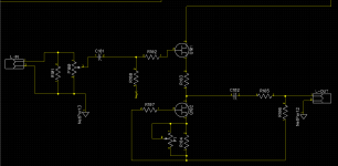
So this is the new version with source resistors. I remember ,last time it came up it was recommended to use a trimpot to null the DC offset.Please see the schematic attached and especially pin connection for trimpot. source resistors are 3ohm (R103) and R104, 3.3 with P1 200ohm pot in parallel.
So this is the new version with source resistors. I remember ,last time it came up it was recommended to use a trimpot to null the DC offset.Please see the schematic attached and especially pin connection for trimpot. source resistors are 3ohm (R103) and R104, 3.3 with P1 200ohm pot in parallel.
Attachments
Yes. But you don't need to use a simulator to tell you that.
I would swap C102 with R105.
Place R105 close to the output node.
Why are you taking the input resistor R108 to the negative power supply?
It is in the signal circuit and should remain solely in the signal circuit.
NetProt3 should connect to neg and then to NetProt2. None of these should be taken to some remote arbitrary "ground". Remember the rule: use LOW LOOP AREA close coupled pairs for all signal wiring. That applies just as much for traces as it does to wires. The difference being you cannot easily twist traces to help with attenuation of EMI, making it all the more important to maintain close coupling.
Andrew , Neg is not a negative , it is the circuit part in B1 that is biasing gate of upper Jfet with half voltage of 18V through 1Mohm resistor Sorry for the confusion.
Last edited:
That's true, it is positive +9V. What does it do ? I have seen some designs with no such biasing?
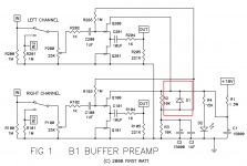
The B1 used an 18Vdc supply in single polarity mode. The DCB1 used a 20Vdc supply in dual polarty mode, effectively +-10Vdc
The B1 requires DC blocking capacitors at both the input and output.
Then the input is biased to ~ half supply voltage. That allows the input signal to swing up (+ve) and down (-ve) relative to the bias voltage without getting close to the supply rails.
Similarly the output swings up and down, again without hitting the supply rails.
No, that is not what was said.
The 18Vdc supply limits the absolute maximum signal swing to 18Vpp.
But in practice the output will be 1 to 2volts less than each supply rail.
So instead of getting +9Vpk and -9Vpk the amp will have a maximum swing into normal loads of ~ +-7Vpk to +-8Vpk for a total swing of 14Vpp to 16Vpp.
If you use nearly all of that into a single ended Follower you will see gross distortion of the waveform. Try looking at a scope plot of a very high level signal.
When the signal only uses ~ 50% of the maximum swing you will find that the distortion is a lot less. Almost invisible on the scope sinewave.
That's puts the maximum low distortion output at ~8to 9Vpp or about 3Vac for an 18Vdc supply into a high impedance load.
If you are processing a CDP signal with a maximum of 2Vac to 2.4Vac, your signal is well below that 50% of absolute maximum. The result is that even on the transients you should not hear any 2nd harmonic.
At average levels of 20dB below maximum (i.e. ~0.2Vac to 0.24Vac) the added 2nd harmonic distortion is completely inaudible. Measurements and FFTs should show it.
Thanks Andrew. What is the role of D1?😀
What is the ideal Cap value for input caps, is it 1 UF or is it 10?
didn't you look closely at sch that you posted and may be able to arrive at the answer??? i am sorry if you are asking something else.... enlighten me..
- Home
- Amplifiers
- Pass Labs
- B1 Buffer Preamp