> You use 'em naked, no buffer resistors, right?
Yes.
> 10K Z ladder pot, LDRs, or multitap Tx volume?
LDRs.
Yes.
> 10K Z ladder pot, LDRs, or multitap Tx volume?
LDRs.
Hi,
If one was to use J310 j-fet rather than K170, what would the preferable source resistor values be? I looked on J310 datasheet and Idss for this device is between 24(min) and 60 (max) mA which is quite a lot. I am asking this because I am playing again with B1 buffer blocks but only have J310 devices at hand...
Thanks 🙂
The B1 is a Pass design that he has kindly passed on to us.
Change the devices and it is no longer a B1.
It becomes a jFET buffer.
Change the devices and it is no longer a B1.
It becomes a jFET buffer.
True, but Papa always gave us a freedom to be creative, "adjust to taste" and modify designs to better suit our needs. No, it won't be the B1, but whatever it becomes, credit goes to Nelson. I just wanted to help myself by accommodating the device I have in the drawer!😎
Guys:I have my B1 buffer driving my 6AS7 SET. Though power is down the detail and tonal texture has never been so high.
I'm right in the middle of a BoZ. But the simpler BoZ. Some things I am taking with me are 2 X 10,000uf of filter caps (snubbed with .1uf poly) separated by 10R. Snubbed output 10uf poly and copper coated tinned copper hook-up wire. Once more I will use the Hammond black anodised Al case.
I badly need some gain. My B1 may go from 5Hz to 780khz and be able to swing 18V into 10K but only 85% of the signal gets through.
The B*ast*ard* son of Zen may be a combo of BoZ and B1 called BBoZ (BeBoZ)??
Last edited:
6AS7 SET is very hard to push even with 18V swing. Any pre-amp tube section before 6AS7?
JFET BOZ has too much gain for my F5 diy clone, but it may be good for you.
JFET BOZ has too much gain for my F5 diy clone, but it may be good for you.
6AS7 SET is very hard to push even with 18V swing. Any pre-amp tube section before 6AS7?
JFET BOZ has too much gain for my F5 diy clone, but it may be good for you.
That's good to know, I'm using B-1 with F-5, and would like more gain, and to that end, am building BOZ on the boards I bought in the 90's. How is it "too much?"
Russellc
6AS7 SET is very hard to push even with 18V swing. Any pre-amp tube section before 6AS7?
JFET BOZ has too much gain for my F5 diy clone, but it may be good for you.
A 12AX7 drives the 6AS7. But I need a high gain preamp to get near the full 3W from the amp. The B1 from my low output Oppo 980H does not produce enough swing to get good volume levels on quiet CDs.
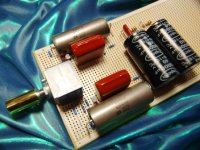
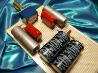
BoZ cct. brd.completed.
See imges below. Once again I used the Russian 0.1uf PIO, and 10uf poly (input cap and output cap respectively) (snubbed with 0.1uf ploy). All on vero-brd. spare central tracks shorted to ground to act as a gatherer. Alps blue velvet 25k pot and slim solid brass knob.
PS: 1R0 to 10,000uf cap, 10R0 to second 10,000uf cap. 5% WBT silver solder used. This will go into a Hammond anodised Al case.
OK it's off thread but strangely related. See U on the BoZ thread.
Attachments
Last edited:
B-1 Build Help Questions
Hello everybody- This is my first post so be gentile. I am new at this and have a few questions regarding the B1. I have read most of the previous posts but have not come across a few questions I have.
1-I plan to use a battery power supply and read I can leave out R1 and C1. My question is can I also leave out C3? If so, do I have to bypass it with a piece of wire or leave it open?
2-Will I possibly have turn on and/or turn off thumps” or other noises by leaving out the above parts and using a battery power supply?
3-In the C100 and C200 position I plan to use caps with 18 gauge leads. I have seen pictures of finished builds with various types of caps (other than the Vishay square caps) in these positions. How do you get these leads through the holes on the pass board?
Thank you very much
David
The B1 is a single ended ClassA circuit.1-I plan to use a battery power supply
It passes high quiescent current all the time. Expect current draw to be ~8mA per channel.
I would plan for using rechargeable batteries for the 18V supply.
Batteries do need a capacitor for decoupling the high current demands at peak transient signals.
Has a class A circuit like that peaks even if it has a constant 8mA current consumption all the time?
My B1 draws just under 20mA at 18V. Usually Class A does not have current peaks.Has a class A circuit like that peaks even if it has a constant 8mA current consumption all the time?
So a decoupling capacitor would be advised to filter RF stuff from DC rather than local energy strorage?
where do you Members read your science?
A B1 at quiescent (no signal) draws ~Idss of the CCS transistor from the supply.
Let's assume we chose a 8.0mA Idss device for the lower FET.
Let's further assume we chose a 8.01mA device for the upper FET.
Now apply the 18V single polarity supply to the pair of series connected FETs.
The lower FET does not have 10V across it and it's Tj will not be 25degC. This tells us that the CCS may not pass exactly 8.0mA. It could be 8.0+-0.2mA depending on temperature and transconductance @ the quiescent current.
The upper FET will probably be passing about Idss or maybe just a tiny fraction less than Idss. The Vgs when the Iq=Idss is zero Vgs.
When the Iq<Idss the Vgs is a -ve voltage. This negative voltage is the output offset. The closer the upper device Iq is to Idss the lower is the output offset. That's why we can use selected Idss FETs, to minimise output offset. In a B1 output offset is blocked and so precise selection of FET Idss is not quite as important. But Pass has designed this circuit to sound good when Iq is almost exactly 100% of Idss.
Now let's apply an AC signal to the upper gate.
This varies the Vgs and thus control the output voltage by varying the effective impedance of the upper FET.
When signal is +ve the Vgs moves to a +ve voltage and more current tries to flow from the 18Vdc Supply rail through the upper FET.
This extra current has two exit routes.
a.) through the CCS FET
b.) through the load.
When signal is -ve the Vgs moves to a -ve voltage and less current tries to pass from the 18Vdc Supply rail through the upper FET.
The CCS FET is still trying to pass it's fixed CCS current value.
The only route for current into the CCS is from
c.) through the upper FET
d.) through the load
On -ve signals the CCS draws (sinks) current from the Load and the Upper FET.
On +ve signals the Upper FET sources current to the Load and the CCS FET.
The signal varies (modulates) the supply rail current by the amount of current that flows in the load. Zero signal in the load (quiescent state) resulting from Zero modulation of the Supply rail current.
Big signal in the load resulting from Big modulation of the Supply rail current.
Peak current in the load could be due to minimum current from the supply rail or from maximum current in the supply rail.
What is certainly not true is that
Learn how circuits operate or for ever be consigned to simply copying exactly proven working designs like any school kid could do.
A B1 at quiescent (no signal) draws ~Idss of the CCS transistor from the supply.
Let's assume we chose a 8.0mA Idss device for the lower FET.
Let's further assume we chose a 8.01mA device for the upper FET.
Now apply the 18V single polarity supply to the pair of series connected FETs.
The lower FET does not have 10V across it and it's Tj will not be 25degC. This tells us that the CCS may not pass exactly 8.0mA. It could be 8.0+-0.2mA depending on temperature and transconductance @ the quiescent current.
The upper FET will probably be passing about Idss or maybe just a tiny fraction less than Idss. The Vgs when the Iq=Idss is zero Vgs.
When the Iq<Idss the Vgs is a -ve voltage. This negative voltage is the output offset. The closer the upper device Iq is to Idss the lower is the output offset. That's why we can use selected Idss FETs, to minimise output offset. In a B1 output offset is blocked and so precise selection of FET Idss is not quite as important. But Pass has designed this circuit to sound good when Iq is almost exactly 100% of Idss.
Now let's apply an AC signal to the upper gate.
This varies the Vgs and thus control the output voltage by varying the effective impedance of the upper FET.
When signal is +ve the Vgs moves to a +ve voltage and more current tries to flow from the 18Vdc Supply rail through the upper FET.
This extra current has two exit routes.
a.) through the CCS FET
b.) through the load.
When signal is -ve the Vgs moves to a -ve voltage and less current tries to pass from the 18Vdc Supply rail through the upper FET.
The CCS FET is still trying to pass it's fixed CCS current value.
The only route for current into the CCS is from
c.) through the upper FET
d.) through the load
On -ve signals the CCS draws (sinks) current from the Load and the Upper FET.
On +ve signals the Upper FET sources current to the Load and the CCS FET.
The signal varies (modulates) the supply rail current by the amount of current that flows in the load. Zero signal in the load (quiescent state) resulting from Zero modulation of the Supply rail current.
Big signal in the load resulting from Big modulation of the Supply rail current.
Peak current in the load could be due to minimum current from the supply rail or from maximum current in the supply rail.
What is certainly not true is that
Do your homework.Usually Class A does not have current peaks.
Learn how circuits operate or for ever be consigned to simply copying exactly proven working designs like any school kid could do.
Frustration is starting to sink in. Is it just me or is trying to search at Digikey difficult?
NP mentioned using a 5ohm 3w for R1.
Is there such a thing or have I missed something? Do you have a source for said resistor.
This is my first build where I'm sourcing the parts (an earlier effort stopped when the aggravation to fun ratio went upside down. I'm trying to prevent this from happening again.
Thanks,
Fred Griffith
Adapting the BI Buffer design to be used with a TVC (or LDR’s)
My initial search started on the net because I recently bought a Wavelength audio Mercury Series, single stage, single tube amp that requires a low impedance preamp (less than 600 ohm) according to Gordon.
I have been using a passive Audio consulting TVC with my 45’s very successfully but this doesn’t not well with the Mercury’s parallel feed design.
Thus I have following questions for you:
What changes do I have to make to the BI buffer design to accept the output of the TVC and do away with the pots?
What is the output impedance of the B1 buffer pre-amp?
Ideally I would like about 20 db gain from this design, can this design be optimized for that?
Would a tube based buffer be a better option?
I am a total novice who understands the basic of electronics but not an EE.
Thanks in advance for the enlightening guidance.
Cheers
Ash
where do you Members read your science?
Do your homework.
Learn how circuits operate or for ever be consigned to simply copying exactly proven working designs like any school kid could do.
This is taking a bit of a high hand.
This is a beginners project and many of us are just starting out and copying is exactly what we are doing.
This attitude does nothing positive and works against what I feel is the intent of this thread and the projects creator.
Fred Griffith
Thank you Andrew for your detailed explanation! I understand now many points better.......🙂
where do you Members read your science?
A B1 at quiescent (no signal) draws ~Idss of the CCS transistor from the supply.
Let's assume we chose a 8.0mA Idss device for the lower FET.
Let's further assume we chose a 8.01mA device for the upper FET.
Now apply the 18V single polarity supply to the pair of series connected FETs.
The lower FET does not have 10V across it and it's Tj will not be 25degC. This tells us that the CCS may not pass exactly 8.0mA. It could be 8.0+-0.2mA depending on temperature and transconductance @ the quiescent current.
The upper FET will probably be passing about Idss or maybe just a tiny fraction less than Idss. The Vgs when the Iq=Idss is zero Vgs.
When the Iq<Idss the Vgs is a -ve voltage. This negative voltage is the output offset. The closer the upper device Iq is to Idss the lower is the output offset. That's why we can use selected Idss FETs, to minimise output offset. In a B1 output offset is blocked and so precise selection of FET Idss is not quite as important. But Pass has designed this circuit to sound good when Iq is almost exactly 100% of Idss.
Now let's apply an AC signal to the upper gate.
This varies the Vgs and thus control the output voltage by varying the effective impedance of the upper FET.
When signal is +ve the Vgs moves to a +ve voltage and more current tries to flow from the 18Vdc Supply rail through the upper FET.
This extra current has two exit routes.
a.) through the CCS FET
b.) through the load.
When signal is -ve the Vgs moves to a -ve voltage and less current tries to pass from the 18Vdc Supply rail through the upper FET.
The CCS FET is still trying to pass it's fixed CCS current value.
The only route for current into the CCS is from
c.) through the upper FET
d.) through the load
On -ve signals the CCS draws (sinks) current from the Load and the Upper FET.
On +ve signals the Upper FET sources current to the Load and the CCS FET.
The signal varies (modulates) the supply rail current by the amount of current that flows in the load. Zero signal in the load (quiescent state) resulting from Zero modulation of the Supply rail current.
Big signal in the load resulting from Big modulation of the Supply rail current.
Peak current in the load could be due to minimum current from the supply rail or from maximum current in the supply rail.
What is certainly not true is that
Do your homework.
Learn how circuits operate or for ever be consigned to simply copying exactly proven working designs like any school kid could do.
Thank you Andrew for your detailed explanation! I understand now many points better.......🙂
Sawdusttt,many of us are just starting out and copying is exactly what we are doing.
did you take the time to explain why their comments were completely misleading?
Did you do anything to help beginners understand the circuit operation?
Did you want beginners to be led astray?
That erroneous message has been repeated in this Forum many times and many times the correct explanation of the ClassA operation has been explained.
Learn to read!
Do the research.
Be informed.
Make informed decisions.
Last edited:
- Home
- Amplifiers
- Pass Labs
- B1 Buffer Preamp