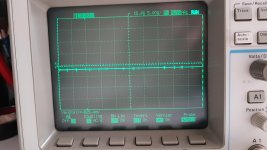
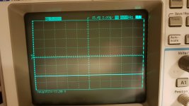
There is no signal, just a -DC voltage (probes in 10x)
On LM319 Pin12 -625mv
On the input via from the driver board 100mV
On LM319 Pin12 -625mv
On the input via from the driver board 100mV
Attachments
Last edited:
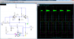
Post the signals on pins 4 and 5 of the 319 with DC coupling. set the scope to 5v/div and whatever timebase it takes to display about 3 complete cycles on the display.
There are no drives/cycles without RCA signal, only on Pin5.
Photo 1 Pin12
Photo 2 Pin4
Photo 3 Pin5
Photo 1 Pin12
Photo 2 Pin4
Photo 3 Pin5
Attachments
Last edited:
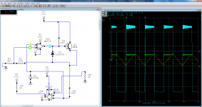
It appears that there is something that's causing the voltage on pin 5 to have offset. I've run it through a simulator. Compare the waveforms to your amp. Do you see significant offset on any other terminals?
Ignore the LM339. The software wouldn't run the 319.
Ignore the LM339. The software wouldn't run the 319.
Attachments
Oh wow, thank you very much for the effort Perry. I really appreciate it 🙂
I was probing around to seek for DC offset causings, but Pin5 seems to be very healthy, nothing has strange readings and it seems to function properly.
I found out the secondary GND is at 4.6v referenced to PS GND.
LM319 Pin5 reads close to 0V when I DC measure with my multimeter between secondary GND and LM319 Pin5.
Should I solder my oscilloscopes reference GND to secondary GND and make new photo's?
I expect LM319 Pin4 to have a negative offset in this case.
Does RK on the lower right of page 4 connect between the grounds?
If not, try connecting then with a jumper.
If not, try connecting then with a jumper.
Resistor RK is not connected between secondary and PS GND.
I referenced the scope to secondary GND.
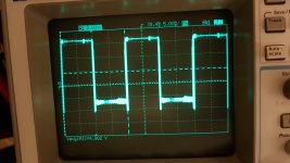
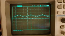
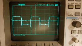
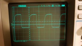
Photo 1 is Pin5 with signal
Photo 2 is Pin4 with signal
Photo 3 is Pin12 with signal
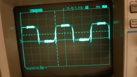
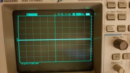
Photo 4 is Pin5 without signal
Photo 5 is Pin4 without signal
Photo 6 is Pin12 without signal
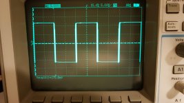
This seems to make more sense, and doesn't look too bad I suppose. Pin12 is pulled down to -VCC without signal, and has a clean square wave with DC right at GND.
The optocouplers from the driver board were OK, the SMBTA92 driver transistor on the driver board has been changed after the crash.
Resistors have been checked.
I referenced the scope to secondary GND.
Photo 1 is Pin5 with signal
Photo 2 is Pin4 with signal
Photo 3 is Pin12 with signal
Photo 4 is Pin5 without signal
Photo 5 is Pin4 without signal
Photo 6 is Pin12 without signal
This seems to make more sense, and doesn't look too bad I suppose. Pin12 is pulled down to -VCC without signal, and has a clean square wave with DC right at GND.
The optocouplers from the driver board were OK, the SMBTA92 driver transistor on the driver board has been changed after the crash.
Resistors have been checked.
Attachments

Last edited:
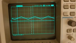
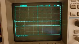
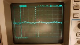
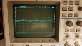
This is a photo from the driver board INPUT via.
With and without RCA signal.
The pull-up resistor R162 reads fine, as well as R161
With and without RCA signal.
The pull-up resistor R162 reads fine, as well as R161
Attachments
Last edited:
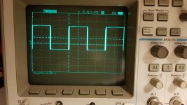
Solder a bridge between pins 1 and 2 of U16. Without input, do you get a triangle waveform on the input of the driver board?
Ahhhaaaa, so that is what IC16 does partially.
I learned a lot from this repair, the troubleshooting and feedback loop, but also the exact creation of a triangle/square waveform.
I don't really directly see in the schematics how soldering Pin1 and Pin2 together makes the output switching go really fast, but I try to understand it later.
On the input via is not directly a triangle wave, but a high frequency switching.
Attachments
If you drive a signal into the amp, do you see modulation on the input?
Using the secondary ground, what points do you see on the 319 that are not within about 0.2v of the audio ground? No need for photos. Just check with a meter.
Using the secondary ground, what points do you see on the 319 that are not within about 0.2v of the audio ground? No need for photos. Just check with a meter.
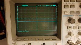
There is a high frequency like in post #137, but at 10-20Hz of RCA input I can't see any modulation in the square wave.
Pin 3 is 11.41v
Pin 9 is -11.41v
Pin 11 is 11.87v
Thats it
Pin 3 is 11.41v
Pin 9 is -11.41v
Pin 11 is 11.87v
Thats it
Re-check. Look at the pins that are connected to the two supply voltages, as well. They are at the upper left of the diagram for the 319.
- Home
- General Interest
- Car Audio
- Audison SR1Dk output driver card, no High-side output