Mauro, thanks.
I'll need to read up a bit.. I remember something about the I2S to PCM negating limits or impact on Fs for the non-os chip.. give me a day or two.. it was one of Ians posts to this thread (probably take that long to find it!!). But it might not be so simple as would the case I2S fed 1541A.
If Ian is around somewhere?.. can send beer via paypal 🙂 !! ?
Shane
FIFO power usage
Hi. I searched the thread for power usage estimates for the FIFO board. The manual recommends 500mA. But a post of measurements measured much lower for the individual components. Ian later corrected these posted FIFO measurement saying it wsa closer to 80mA. My SI clock board is powered by a LiFePO battery.
Was there a more updated actual measurement of power usage? Does the 500mA in the manual correspond to a 2x overhead of the actual usage?
Sorry if this was answered before, but in a couple of hours of searching I didn't find it 😱...
Are people using shunts to power the FIFO board setting up their shunts for 500mA because the overhead is already built into the 500mA number, or are the shooting for 600-700mA? Or 300mA is more than enough based on the measurements mentioned before?
Thanks in advance.
Hi palmito, how are you doing?
The real measured current of FIFO(only) was 80mA @24/24MHz MCLK. It could be a bit more for higher MCLK. The recommendation was by considering applications with clock board powered by FIFO, plus room for safe.
So, I can say to power FIFO with 300mA would be more than enough in this case.
Regards,
Ian
Doing well Ian, thanks for asking! Hope you too are doing well.Hi palmito, how are you doing?
As always, thanks for the quick support, stay safe!So, I can say to power FIFO with 300mA would be more than enough in this case.
Dual XO II clock board
Got Dual XO II PCB samples the day before yesterday. Busy assembling prototypes. Will do test and evaluation this weekend. Will post something very soon.
Have a good weekend.
Ian
Got Dual XO II PCB samples the day before yesterday. Busy assembling prototypes. Will do test and evaluation this weekend. Will post something very soon.
Have a good weekend.
Ian
Last edited:
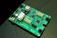
New Dual XO II clock board prototype (1)
It took me three evenings to assemble three Dual XO II prototypes 🙂. Too many SMT components on both sides.
There are many improvements on new Dual XO II. I’ll list them one by one.
It’s the first clock board which can support XO frequencies from 11.2896 to 98.3040MHz, including OCXOs and external oscillators . So, with it, we can play with a large variety of XOs to have more fun.
Firmware was upgraded for more smart. Different frequency XOs can work together at same time. No jumper is needed any more for frequency selection. They can be recognized automatically.
Ian
Attachments
Last edited:
New Dual XO II clock board prototype (2)
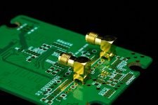
To make it optimized to low jitter in such big frequency range, I have no choice but to use four layers PCB, though the cost can be increased a little bit.
SI performance will be much better than two layers, such as impedance control of high frequency signals, lower power supply noise, whole GND plate and many others.
Ian
Attachments

Ian,super board and photos. I like also soldering very clean
Thanks clsidxxl,
After assemble all SMT components (before connectors), I just put the board into a small zip bag with some isopropyl alcohol for 5 minutes. The board will become very clean. And you just need very small amount of alcohol.... My another secret 😀
Regards,
Ian
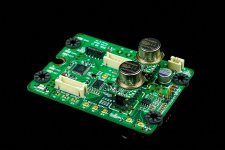
New Dual XO II clock board prototype (3)
Besides standard DIP XO sockets, two SMT XO footprints are reserved on the new Dual XO II clock board. So we can solder SMT XOs, such as CCHD957, CCHD950 or 5X7 and other sizes, directly onto the PCB to eliminate negative DIP pins.
Two SMA input connectors are also reserved to work with high quality external XOs. However, if you want to have both kinds of standard DIP socket and SMA connector to work with different XO solutions, you can assemble SMA connectors at back of the clock board. In this case, SMA connectors have to be soldered first. Right angle SMA connector would also be recommended to save space under the clock board.
You might already be noticed that all reserved XO connections are sharing same clock pin. It could be possible to place them separately at different position, but I jute don’t want to do anything which can probably degrade the quality of clock signals.
Ian
Attachments


Last edited:
Thank you very much Ian.
So,for meet my project (with Isochrone OCX external clock 16/44 -24/192)
the High frequency SMD x2 (the best one of CCHD957, CCHD950 or 5X7 ) .
with Right angle SMA connector may be my choice.
So,for meet my project (with Isochrone OCX external clock 16/44 -24/192)
the High frequency SMD x2 (the best one of CCHD957, CCHD950 or 5X7 ) .
with Right angle SMA connector may be my choice.
Hi Ian,
Do you plan a FIFO production again with the new clock board ?
Did you benchmark Crysteq vs NDK à la DIYinkh website ? Crysteq stays better ?
I really enjoy the I2StoPCM board 🙂!
Do you plan a FIFO production again with the new clock board ?
Did you benchmark Crysteq vs NDK à la DIYinkh website ? Crysteq stays better ?
I really enjoy the I2StoPCM board 🙂!
How about 8 channel out???
Multi-channel I2S/DSD FIFO is my another project which is still under R&D. Hopefully I can finish it in Q2 of this year.
Ian
Hi Ian,
Do you plan a FIFO production again with the new clock board ?
Did you benchmark Crysteq vs NDK à la DIYinkh website ? Crysteq stays better ?
I really enjoy the I2StoPCM board 🙂!
Hi Eldam,
Yes I will 🙂. Probably also went to upgraded it to FIFO II 😀
I have both CCHD957/50 and NDK, listen to Crystek more. But most OCXO recently.
Regards,
Ian
- Home
- Source & Line
- Digital Line Level
- Asynchronous I2S FIFO project, an ultimate weapon to fight the jitter