FifoPi with I2S/DSD/Dop to HDMI converter board(HDMIpi)
FifoPi works together with HDMIpi through u.fl cables to convert MCLK and I2S/DSD/DoP into HDMI LVDS
Can setup an ultra low jitter HDMI transport.
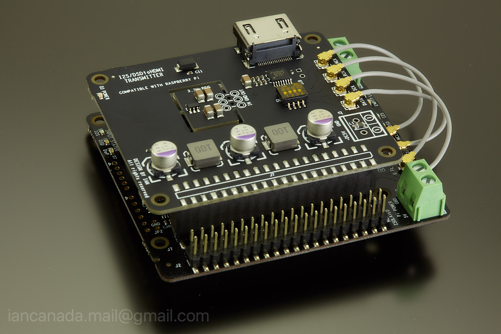
HDMIpiFifoPi by Ian, on Flickr
FifoPi works together with HDMIpi through u.fl cables to convert MCLK and I2S/DSD/DoP into HDMI LVDS
Can setup an ultra low jitter HDMI transport.
HDMIpiFifoPi by Ian, on Flickr
Maybe read the documentation which has a table with clock values?
I just opened the document and saw the table. Will try to understand. Thank you.
hi all,
I am absolutely new to the digital realm but I really want to improve my RPi3.
My system is as followed:
RPi3 model B+ (Linear PSU)/Moode audio v5.0 : AGD NOS19 DAC (PCM1704 basic model) : Preamp : Active speakers.
I read the documents and I think I will need:
1. FifoPi Ultimate board, CCHD957daapterKIT, U.FL cables(how many?),
2. Take away the 2 stock OXs and install CCHD957 clocks(get those from mouser.com myself?) and solder them on the CCHD957daapterKIT and solder the whole thing onto Fifopi....?
3. Do I need a special cable with one end-U.FL and the other end like AES for my AGD dac?
I also have a second system:
RPi3 model B (Linear PSU)/moode audio v3.84 : Soekris dam1021 Dac : Preamp : Active speakers.
Do I need the Fifopi board for Soekris Dac? I read somewhere that frequency switches automatically and no need for better clocks.
Also, will the LifeO4 power supply kit be good for Soekris Dac or my AGD Dac and rpi3?
Thank you for helping me, the clueless newbie!
I just opened the document and saw the table. Will try to understand. Thank you.
FIY fs is 44100 or 48000 Hz and 64*fs is DSD64 so pick a clock that would allow you to play the files you have (or if upsampling the rate you want to upsample to). A 45/49 MHz combo will allow you to play anything up to DSD512 but if you only have CD rips at 44100 Hz (and don't upsample) you can get the lowest frequency clock listed in the table.
Hi there.
I'd need some advise. I am in the process of tweaking the FifoPi.
A friend of mine sent me a pair of these tiny NDKs for the FifoPI.
Do I recall it correctly that somebody somehow installed these tiny NDKs without using the socket plus adapter?
If so, how would that be done?
If that wouldn't work, I guess I'd need the socket and adapter.
Thx
SC
@soundcheck
IanCanada's Latest RPi GB Goodies Impressions... and your tweaks, mods and hints...
I found the cap over the top didn't work though!
IanCanada's Latest RPi GB Goodies Impressions... and your tweaks, mods and hints...
I found the cap over the top didn't work though!
I'm sure you know this but for clarity... the socket is already on the FIFO pcb. So I imagine that step 1 is removing the socket from FIFO. step 2 is to solder the NDK chip directly to the FIFO PCB.Hi there.
… If that wouldn't work, I guess I'd need the socket and adapter.
SC
I honestly cannot imagine doing all that without messing up the FIFO or losing the NDK. While there no doubt will be some last % of performance possible by removing the socket, is it worth the risk and effort? Having done this with the acko s03 I must say I really value having the socket available on the FIFO. It is so much easier to remove the adapter and solder away from the full pcb. And as soon as you get comfortable with the NDK, you will want to try something else. The socket makes this a breeze.
I'm sure you know this but for clarity... the socket is already on the FIFO pcb. So I imagine that step 1 is removing the socket from FIFO. step 2 is to solder the NDK chip directly to the FIFO PCB.
I honestly cannot imagine doing all that without messing up the FIFO or losing the NDK. While there no doubt will be some last % of performance possible by removing the socket, is it worth the risk and effort? Having done this with the acko s03 I must say I really value having the socket available on the FIFO. It is so much easier to remove the adapter and solder away from the full pcb. And as soon as you get comfortable with the NDK, you will want to try something else. The socket makes this a breeze.
I hear you. I probably better get me a pair of adapters to begin with.
Do you have a pic how you've done it?
As I said, you need to be comfortable with SMD and have some magnification to do this. I broke up the adaptor socket with side cutters and took it out one pin at a time. It's just a DIL footprint so no problem reinstating it if need be.
It looks a bit gungy because I removed the electrical grade silicone I'd put on the top for damping to take the image. Don't use ordinary silicone, it will eat the components!
Attachments
Last edited:
Looks doable.
Brute force to remove the sockets.
The pads are there.
And plenty of space around to work with a heat gun.
You got me tempted. 😀
No extra cap buffering/decoupling?
Brute force to remove the sockets.
The pads are there.
And plenty of space around to work with a heat gun.
You got me tempted. 😀
No extra cap buffering/decoupling?
@soundcheck
Ian already provided local bypass caps for the 3.3V on each clock on the underside of the board. Likely it is worthwhile to experiment with them, though @simon dart's experiments suggested it may be hard to improve on them.
BUT be warned that he has an array of what I believe are 0402 sized caps there which are difficult to un-solder/solder even if one is VERY GOOD at SMD rework.
Greg in Mississippi
Last edited:
I have no intention to do more then necessary. 😀
Let's hope that the heatgun treatment won't lift off the caps down under.
For sure it's gonna be an interesting operation. 😉
Let's hope that the heatgun treatment won't lift off the caps down under.
For sure it's gonna be an interesting operation. 😉
Let's hope that the heatgun treatment won't lift off the caps down under.
Maybe less risk of board damage it one were to cut away the plastic frame of the socket with small diagonal cutters, leaving only the pins. Any pins that need removing could be heated from the bottom with an iron and pulled out from the top with some needle nose or similar. Or, pins could be clipped off almost flush without removing them.
Can someone point me to the list of the latest offering? I kind of got lost with all these products.
D
D
One more question.
If a better clock gets implemented or simply a better I2S signal is provided
does the Sabre DPLL bandwidth should be adjusted accordingly?
From what I've seen in the datasheet the DPLL default setting is 5 for PCM. There'd be 4 more levels to go for (0 would be DPLL off).
Do I recall it correctly that people reported better performance/SQ with lower DPLL BW settings?
(Assuming that the incoming signal is a rock solid low jitter signal - e.g. FifoPi with clock upgrade.)
Last edited:
@Nikon1975,
Check post 3171 of this thread:
Ian asynchronous I2S and S/PDIF FIFO KIT group buy
Greg in Mississippi
Check post 3171 of this thread:
Ian asynchronous I2S and S/PDIF FIFO KIT group buy
Greg in Mississippi
Do I recall it correctly that people reported better performance/SQ with lower DPLL BW settings?
Yes, the lowest setting that allows for stability usually sounds best. DSD tends to sound better than PCM with these dacs, too.
I read some where that Allo's sparky board is supporting native dsd256 now. Rpi still can't play native dsd256, is it correct? So I am thinking to connect my Sparky with Fifopi and output i2s through u.fl connectors to external dac.
May I know what kind of cable to use to connect GPIO pin from Sparky to GPIO pin at FifoPi? Could you show a pic for the cable and where to get it? I also own an Odroid C2 sbc and rpi 2B sbc.
May I know what kind of cable to use to connect GPIO pin from Sparky to GPIO pin at FifoPi? Could you show a pic for the cable and where to get it? I also own an Odroid C2 sbc and rpi 2B sbc.
Last edited:
Rpi still can't play native dsd256, is it correct?
I assume that depends on the software and interface you use.
- Home
- Source & Line
- Digital Line Level
- Asynchronous I2S FIFO project, an ultimate weapon to fight the jitter