
After long hours sim I believe I finally got a good solution.
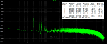
Using a sziklai input transistor (with a very linear pnp 327-40 ) I did reduce THD to acceptable values.
Vin = 1VDC
N-Period=1
Fourier components of V(vout)
DC component:-0.00548786
Harmonic Frequency Fourier Normalized Phase Normalized
Number [Hz] Component Component [degree] Phase [deg]
1 1.000e+03 2.201e+01 1.000e+00 -0.10° 0.00°
2 2.000e+03 3.115e-05 1.415e-06 13.94° 14.05°
3 3.000e+03 3.743e-05 1.700e-06 -105.46° -105.36°
4 4.000e+03 4.096e-06 1.860e-07 -178.72° -178.61°
5 5.000e+03 4.567e-05 2.074e-06 99.93° 100.04°
6 6.000e+03 3.179e-06 1.444e-07 -179.37° -179.26°
7 7.000e+03 5.154e-05 2.341e-06 96.73° 96.84°
8 8.000e+03 3.548e-06 1.612e-07 177.77° 177.88°
9 9.000e+03 2.985e-05 1.356e-06 99.44° 99.55°
Total Harmonic Distortion: 0.000407% (0.000368%)
Attachments
Last edited:
Now I will start the layout and keep posting my evolutions here.
Phase margin is also considerably improved....
Phase margin is also considerably improved....
Attachments
Last edited:
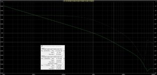
Response looks good with 26.8dB gain @ 1kHz and -3dB @ 405kHz
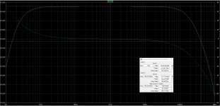
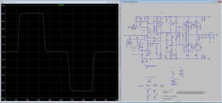
Large signal squares using the highly valuable tool provided by Sandro, looking very good at 1VDC input
Large signal squares using the highly valuable tool provided by Sandro, looking very good at 1VDC input
Attachments
Last edited:
Ricardo,
It looks more consistent and reliable.
It is time to go to assembly a prototype and find real behavior.
If you allow me a suggestion:
Make an simple assembly using cheap commercial pre fabricated standard board.
It is easy to change and define solution to other problems that came with parts variation related to model.
Regards
Ronaldo
While studying the small step response I realized some spikes in the input current of the vas so I increased IPS current, reduced the miller cap and removed the Clead cap.
Now transient response is much better but I lost some degrees phase margin that now sits at 52° with 19dB gain margin.... still looking good.
Now transient response is much better but I lost some degrees phase margin that now sits at 52° with 19dB gain margin.... still looking good.
Hi Ronaldo
Yes, it looks better and sims better also.
I will now proceed with the layout so when I can I will buy some proto boards.
Yes, it looks better and sims better also.
I will now proceed with the layout so when I can I will buy some proto boards.
Ricardo
It looks normal and it is the reason to lots of comments in forum saying that small THD in simulation do not means a good sounding real amplifier.
Simulation also give you lots of information about amplifier circuit behavior and help to troubleshoot real amplifier.
All theses parameters are related and a really good amplifier has perfect square wave response (or step response) and low distortion.
Another point is related with amplifier output current capability (output stage and power supply are the point of study here).
To finish, an real frequency response of at least 200KHz under output load is the last amplifier point to check.
If you are interested try to simulate really good amplifier try Sansui Alpha to see all I write to you. Model AU-Alpha907mr.
For test purpose I suppose you have and oscilloscope, a square wave generator and a resistive dummy load. Is very dangerous connect an amplifier under test to a good speaker.
Proto board is good to low power circuits, not to amplifier that deal with high currents and voltages. The best in this test is use perfored standand boards (sorry I do not remember the correct name in english) and make solders point to point
With kindest regards
Ronaldo
Last edited:
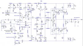
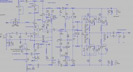
The latest schematic with JFET CCS.
Please note that Vds in J1 is a meagre 1.33V.... I will try to find a k170GR with very low Idss so Vp is also minimized and maybe I can get away with it.
This version presents better distortion characteristics than the previous one using LED/BJT CCS.
IMO k170 CCS sound good in other applications (phono stage and shunt vref) so it should be a good choice here.
Tried to use a stiffer cascode CCS instead of J1 but could not make it work ... Maybe you guys could drop in and try to improve on this matter....
Attachments
It looks normal and it is the reason to lots of comments in forum saying that small THD in simulation do not means a good sounding real amplifier.
I agree. Small distortion is not enough, I prefer monotonic harmonic profile also.
Ricardo,
I count 14 transistors plus the outputs for a power perhaps 145W?
You have a commendable THD but at high output you have a high level of H5, less than 10dB below H2.
This amp will sound clean but a little sharp because of this H5 artefact.
Although a good amp it seems to be over complex. You should be able to do a very good amp using a singleton input stage with no more than four transistors plus the outputs.
If you use the ECW20N/P20 series of Exicons, you get double die with 200V, 16A, gm of 1.4 and 250W.
Finally, a bias gen for laterals need only be a resistor and a cap. Run the outputs around 200mA quiescent and they will always drop slightly at higher levels - foolproof.
Very good VAS transistors are 2SC2682 and 2SC3503. They have pnp matchers and their speed, Cob and cost are very reasonable. If you run these transistors at 15mA there is more than enough drive to shake the gates of the laterals. You will need heatsinks, however, THM Aavid 6030 series, 16C/W.
Hugh
Thank you so much Hugh
Will continue my pursuit following your input.
I will start with the ECW20N/P20 series.. then search for the 2SC2682 and 2SC3503.
PS: In this case I am using VR2 R17 for mosfet bias with the // cap C13 so I believe this is ok
So you suggest I run the Vas at 15mA and drop the complex floating CCS and mirrors.... Will do that also...
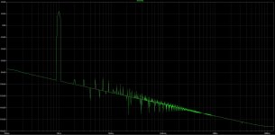
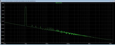
It has a monotonic harmonic distribution at high frequencies..... At 1khz full power (150W) it looks like this:
+1000
Ricardo,
One thing I've noticed in LTSpice when running sims for FFT plots on designs that include power supply bypass caps... I have to insert a small resistor immediately after the voltage source and before the first bypass caps. I use something like 0.01Ω. Without this, I can never get the FFT noise floor to settle out. If I add these are run the sim with a 2 to 3 second delay, it will settle out at -240 dB.
One thing I've noticed in LTSpice when running sims for FFT plots on designs that include power supply bypass caps... I have to insert a small resistor immediately after the voltage source and before the first bypass caps. I use something like 0.01Ω. Without this, I can never get the FFT noise floor to settle out. If I add these are run the sim with a 2 to 3 second delay, it will settle out at -240 dB.
Thank you brian will test this asap. Just one question.... the longer the sim, the lower thd results right ?
Not in my experience. Overall THD doesn’t change materially, but the phase angle of the harmonics and FFT plot do change significantly.
Brian,
You can introduce an impedance into the power supplies; I use a very poor 0.2R to assess the clipping performance and THD.
This is my tran line: .tran 0 {simtime} {dlytime} {timestep}
And my command lines:
.options plotwinsize=0
.options method=gear
;.step temp 0 60 10
.options numdgt=7
.param freq=1k
.param numcyc=10
.param dlycyc=5
.param FFT=2**16
.param simtime=numcyc/Freq+dlytime
.param dlytime=dlycyc/Freq
.param timestep=(simtime-dlytime)/FFT
.four {freq}15 8 V(Vout)
.four {freq} 4 8 V(Vout)
This seems to be very good and gives very accurate FFTs and reasonable THD. It allows the same cycle waveform length and consistent THD analysis regardless of frequency.
Hugh
- Home
- Amplifiers
- Solid State
- Assemblage Power Amp