Those are voltage regulators for the output stage power supply.
They are also in part 2.
😎
Thanks Mr Pass
Fantastic 🙂
IRF To-3's recorded in BOM list.
Greetings
Attachments


Thanks Mr Pass
Fantastic 🙂
IRF To-3's recorded in BOM list.
Greetings
The bottom left corner of the hieroglyphic schematic was signed Pharaoh Pass.
Let's shorten the wait by gnawing on this onePeople is starting to see visions with this long wait.....
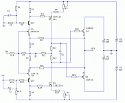
k170/j74 form an input stage cascoded with Q12/Q13 driving k2013/j313 loaded with R12 (R13/R16 are part of the load but their main purpose is to set Vgs value for VFETs). C2 equalises the AC potential at VFETs gates and the F5-like feedback (R24/R3 and R23/R2) network sets the gain. P1/P2 set DC offset at the output and bias current.
Schematic lacks values because they heavily depend on actual properties of semiconductors used - my prototype has input JFETs of BL grade (Id = 6.5 mA at Vds=9.5V), k2013/j313 have Vgs of 2.3V at Id=45mA and VFETs exhibit Id of about 1A at 10-11V Vgs.
Input/Vas PS voltage can be lower - with +/-50V I can get more than 30V of clean swing at the VFETs' gates which is not needed (unless I had more than 1 pair per channel).
With few more pairs of VFETs the circuit could work beautifully even without feedback loop but since I got just 2 pairs I had to use feedback in order to lower the output impedance.
So far I like it but I need to check how it's different from the same input/VAS with lateral MOSFETS at the output (as soon as the "buying a second-hand car in Berlin" drama finishes)...
Attachments
Let's shorten the wait by gnawing on this one
k170/j74 form an input stage cascoded with Q12/Q13 driving k2013/j313 loaded with R12 (R13/R16 are part of the load but their main purpose is to set Vgs value for VFETs). C2 equalises the AC potential at VFETs gates and the F5-like feedback (R24/R3 and R23/R2) network sets the gain. P1/P2 set DC offset at the output and bias current.
Schematic lacks values because they heavily depend on actual properties of semiconductors used - my prototype has input JFETs of BL grade (Id = 6.5 mA at Vds=9.5V), k2013/j313 have Vgs of 2.3V at Id=45mA and VFETs exhibit Id of about 1A at 10-11V Vgs.
Input/Vas PS voltage can be lower - with +/-50V I can get more than 30V of clean swing at the VFETs' gates which is not needed (unless I had more than 1 pair per channel).
With few more pairs of VFETs the circuit could work beautifully even without feedback loop but since I got just 2 pairs I had to use feedback in order to lower the output impedance.
So far I like it but I need to check how it's different from the same input/VAS with lateral MOSFETS at the output (as soon as the "buying a second-hand car in Berlin" drama finishes)...
Hello juma. Is your schematic modifiable so as to include a transformer like Mr. Pass showed in his concept CSX2 amp?
Let's shorten the wait by gnawing on this one
That's nice looking, and certainly simpler than mine.
😎
Could you please provide the link/schematic ?
First article in Firstwatt website.
Why not show directly on step to give a reference? Camon this is a entertainment place. not the lunge thread.
Thanks,That's nice looking, and certainly simpler than mine.
😎
it's inspired by your previous work. The PSU is more complicated than the amp (all four rails regulated, made from two 22V AC secondaries)
Yes, the transformer can be used to drive the VFETs but since they are used here as source followers you'll need much better (more expensive) transformer that is able to deliver much higher voltage swing. Ergo, it's doable but I don't see any advantage in doing so...First article in Firstwatt website.
Last edited:
Why not show directly on step to give a reference? Camon this is a entertainment place. not the lunge thread.
I do not have the posting skills to implement your suggestion. I got my limitations.
Hello juma. Thank you for your analysis and answer. You already have a great working prototype; which is amenable for possible practice by other DIYers. I rest my questions.
Always happen that a cool engineer came with smart references and ruin the thread. All the people in the Diy world waiting for the new pushpull from the guru, eating ours owns nails and just arrive a new cow to the ranch illuminating the thread with idiots ideas sending every body for get the references and with lazy attitude, doesn't give any more than their owns egomaniacs answers. Them also are Avoiding give a light in the mind. I don't know what is worst, wait for the project that never arrive or continue supporting that kinds of brainless.
😎..me i was hoping Juma's provocation would move Papa NP to publish ...but nothing will deviate him from his path of publishing only when he is happy with the results of what he's got.
Thank God for that.
As usual i know it will be worth the wait....my Sony's are waiting.....😀
...this prompts a though: why is it that the less time you have in life the more you are willing to wait for something worthwhile ?
..ZEN moment ....😎
Thank God for that.
As usual i know it will be worth the wait....my Sony's are waiting.....😀
...this prompts a though: why is it that the less time you have in life the more you are willing to wait for something worthwhile ?
..ZEN moment ....😎
Last edited:
Juma has given you the gist of it.
Finished piece will have cherry on top.
😎
😀 Yes...but who was the Architect that said : " the devil is in the details"
...just enjoying the discussion....😉
'sides it is always exciting to read a new article from you.

Last edited:
Attachments
Always happen that a cool engineer came with smart references and ruin the thread. All the people in the Diy world waiting for the new pushpull from the guru, eating ours owns nails and just arrive a new cow to the ranch illuminating the thread with idiots ideas sending every body for get the references and with lazy attitude, doesn't give any more than their owns egomaniacs answers. Them also are Avoiding give a light in the mind. I don't know what is worst, wait for the project that never arrive or continue supporting that kinds of brainless.
Your style of writing has an admirable sense of humor. I forgive you for ascribing me the above unpleasant human qualities.
- Status
- Not open for further replies.
- Home
- Amplifiers
- Pass Labs
- Article - Sony VFETs part 1