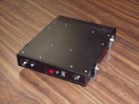
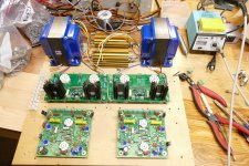
I have done PC board layout for everything from a simple tube or solid state audio amps to cell phones, police walkie talkie,s and high powered mobile radio transceivers. The trunk mounted 700 MHz LTE based transceiver seen in the first picture put out 100 watts of peak RF power from a 12 volt car battery peak currents were in the 20 amp range. Yes, this one used 2 Oz copper, and lots of it in the 28 volt boost converter and RF power amp. I used Mentor Graphics PC board tools for that design. Here each routed signal was assigned to a routing class, each with its own design rules. Trace width, spacing, and layer restrictions are put in place for each routing class before the PC board layout is started and the rules are enforced by the layout software.I'd like to see George Anderson, aka Tubelab chime in. I pretty much copy what he seems to be doing with PCB sockets directly on the boards.
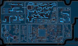
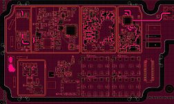
A similar situation exists, but at the other end of the layout spectrum occurs when trying to stuff 600 components into a small PC board for a police walkie talkie. The blue and red pictures show the outer two of the 10 layers used in this prototype board. Two layers are solid ground except for the keepouts for the through holes.
PC boards for tube amps are far simpler than either of these. There are three major concerns, and a fourth that I have self imposed.
Tube amps involve high voltage. The plate voltage on the output tube in an audio amp will reach 2 X the B+ voltage in normal unclipped listening and go much higher when the amp is driven to clipping into a reactive load like a speaker near resonance. I have seen 2500 volt peaks in a cranked guitar amp that ran from a 430 volt B+ voltage into a guitar speaker at resonance. Trace SPACING must accommodate this voltage without flashover.
The tube heaters require high current. Here the trace WIDTH is important, especially if 1 Oz copper is used. I tend to stay well within the 4 to 5 amps per 100 mills guidelines provided by the PC board vendors. The fattest sweep tube that I know of consumes 2.65 amps of heater current. An amp with two of them will pass over 5 amps continuously and far more on start up. The UNSET board can use a pair of these tubes, so the short heater traces are 125 mills wide (0.125 inches). The SSE board has been built with 6DQ6 sweep tubes drawing 1.2 amps each, so 100 mil traces were used. The TSE-II uses very wide traces that are doubled up (on top and bottom layers) for low voltage drop.
Use the calculator found here to find the limit of a given trace, and stay well inside it:
https://www.4pcb.com/trace-width-calculator.html
It has been mentioned throughout this thread and most other "PC boards are evil in tube amps" threads that tube sockets should not be mounted directly to the PB board. Plenty of tube TV sets made on crummy phenolic board with cheap sockets set forth a good reason for this belief. Some of the PCB based TV's in the early 60's literally came apart, warped beyond use, and even caught fire due to poor materials and inexperienced designers. Often these boards had poor adhesion between the board material and the copper traces which got worse over time due to heat cycle induced stress. It was not uncommon to rip a socket with some traces attached from the board while attempting to extract a firmly entrenched tube from its socket. This is not necessarily the case today, IF some thought is put into the design and good quality materials are used. There are still plenty of the cheap plastic or phenolic based tube sockets available on the surplus market today. Why would someone make a cheap plastic socket for a TV sweep tube that's going to get HOT. I got some cheap from AES and melted one so they were all trashed. I use only ceramic sockets. Even the cheap Chinese ones are OK as long as you change them after a few hundred tube swaps as the pins get loose.
In order to reduce the chance of issues with PCB mounted sockets I made the pads for the tube socket pins much larger than what's seen in most other PC board designs. All of my tube amp boards use double sided plated through holes for maximum pad to board contact area. This makes it nearly impossible to rip out a pad in a well made board.
I mentioned a self imposed rule that I follow for all Tubelab boards and most anything else where tight spacing is not needed. My boards get sent all over the world. Some are built by seasoned experts, but most are often a "first time build." Many of my own boards, and those belonging to some other users on this forum get used for "experiments" some of which may end badly. To make the board more robust I use no traces thinner than 50 mills and also use a 50 mill minimum spacing. Component spacing is generous for an easy build and an easy repair if needed. This makes the board much more resistant to less than optimum soldering skills. Recently I needed to test some mosfets for use as replacements for the hard to find IXYX IXCP10M45S chip used in the SSE and TSE-II board. I dug through my "box of dead circuits" and found an old well used SSE board which I got working and used for all of this testing. During that session I realized that the board on my bench was the very first SSE board I ever made. It has seen hundreds of tubes rolled through it, dozens of parts changes including at least two sets of output tube sockets, yet other than a coating of permanent dirt and grime, it still looks as it did when it was made over 16 years ago.
Those experiments are here starting in post #26:
https://www.diyaudio.com/community/threads/10m45s.390771/page-2
It is also a good idea to space the components 1/8 to 1/4 inch above the board when building. This allows for improved airflow and makes it far easier to remove the part if necessary.
Attachments

Anything under 2oz copper has issues with removing and replacing parts, from my experience. 1oz might be fine for production with vaporphase reflow for manufacturing, but hand soldering is a bit more demanding on the epoxy and cladding.
I have to love this 29 ga example, but for different reasons I bet. OPT primary wire gage...lots and lots of turns. 120 mA does not make the beast unhappy. None of my voltage amplifier plate loads run that much current.
Now with PCB, I would also prefer more copper. Time spent to design the board, accounting for voltage/creepage/clearance issues is large compared to PCB cost...so bump it to 2 Oz, or more.
Douglas
Now with PCB, I would also prefer more copper. Time spent to design the board, accounting for voltage/creepage/clearance issues is large compared to PCB cost...so bump it to 2 Oz, or more.
Douglas
Anything under 2oz copper has issues with removing and replacing parts,
One of my tasks at Motorola was spending time with rookie engineers that were fresh out of college. I also got elected to teach the entire graduating class of 1993 at Nova Southeastern's college of computer engineering how to solder when I was a student there, as I had been soldering everything from electronics to slot car chassis since my pre-teen years. I found that 1 Oz copper was the sweet spot for inexperienced solderers to learn on when using a typical 40 to 60 watt iron. The heavy stuff pulls too much heat out of the iron leading to cold or brittle joints.Now with PCB, I would also prefer more copper. Time spent to design the board, accounting for voltage/creepage/clearance issues is large compared to PCB cost...so bump it to 2 Oz, or more.
When laying out a board for Motorola we used a thermal relief, AKA wagon wheel anywhere a component lead or an SMD pad connected to a ground plane or other large area of copper on the board. These make for easier part removal and prevents "tombstoning" on IR reflowed SMD builds. I also found that these lead to ripped out through holes on tube amp boards when a rookie tries to remove a part, so I do not use them. Many people use too much heat and not enough time.
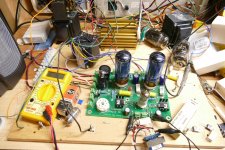
I have been soldering up a little test amp for the past few days. This should be capable of setting many speakers on fire! I have my iron set on 325C. Just how accurate this 25 year old Jameco iron is, I don't know.
Attachments
I seem to remember from electronics classes that electrical flow was mainly on the surface of a conductor. So a thicker wire gave more radial surface area for more current capability. PCB traces have higher surface area to cross section ratio, so this would seem to increase current capacity for same copper cross section. Increased surface area of traces also allows for better heat dissipation, especially if affixed to any type of dissipative material- ie- pcb. I also use Digikey Trace width calc as guide, but defer to .080" min for 800ma heater traces in latest project (below), which taper up .100" then .125" in width through the length of run to the source.
My PCB layouts use 'vias' for tube pins in my software. This notation puts equal sized pads on both sides of double sided pcb, with connecting copper through the hole. This design does make it difficult to replace a socket, which is why I consider a vacuum desoldering station necessary if you're doing any pcb rework.
I attach pcb to chassis at 2 points per tube socket 180* out of phase using the 2 circular relief points on the socket perimeter to tuck in (2) 6-32 screws per socket (shown in pic) with 1/2" alum spacers for offset . These 2 screws are as close to mechanical load point (installing, removing tubes) as possible to reduce board flexing.
Jim
Attachments


3.2mm clearance without copper cladding on both sides as the FR4 isn't going to isolate 500V between the layers.
For me the 900V mosfet leg is too close to the pcb mounted heatsink. I will have to grind some clearance as the back of the mosfet is out.
For me the 900V mosfet leg is too close to the pcb mounted heatsink. I will have to grind some clearance as the back of the mosfet is out.
At DC and audio frequencies the current flow is pretty much evenly distributed throughout the entire conductor. At radio frequencies the RF current does tend to flow along the surface. This is why lots of RF stuff uses silver plated wire, especially in RF inductors.I seem to remember from electronics classes that electrical flow was mainly on the surface of a conductor.
My PCB layouts use 'vias' for tube pins in my software. This notation puts equal sized pads on both sides of double sided pcb, with connecting copper through the hole. This design does make it difficult to replace a socket, which is why I consider a vacuum desoldering station necessary if you're doing any pcb rework.
When I change a tube socket, it's usually because it's worn out. In that case I cut the pins in half right at the base of the socket, then remove each pin individually with tweezers and a soldering iron. I then use a solder sucker and an iron to clear each hole.
I think you answered your own question: Use DC heaters ... or pay attention to your PCB layout. Nobody says you have to run the traces side-by-side. You could stack them. You can reduce the dielectric thickness further by having a 4-layer board and putting the heater traces on layers 3 and 4 and the signal traces on layer 1. 4-layer boards in prototype quantities are pretty cheap these days. I'm not suggesting that this is necessary to do – only that it is an option.Unless dc heater, why would anyone want to spred the ac heatercurrent strayfield with side by side thin and wide conductors?
I've never understood why someone would go through the trouble of making a PCB only to run wires across it. Running wires does not solve the fundamental problem of stray fields coupling into sensitive nodes.
I've designed PCBs for tube circuits with both DC and AC heaters and haven't had any significant hum issues. I aim for below 1 mV RMS of hum at the speaker output. All of my published designs have measured well below that.
Tom
Unless you really want silver, MG Chemicals makes "Liquid Tin". It works pretty well and the surface remains solderable for quite a while.Or we switched to a Tin-base solution? On the US market in the 21st century I find something similar, Silver, called "non-toxic".
Tom
My heaters are AC- But I'd forgotten the phenomenon was frequency related.That's only true at high enough frequencies (skin effect)
Or, in my case, the tube socket outlasts my interest in the current pcb design- So I cut the pcb into segments around the pins w/ a dremel & remove w/ iron... cuz I'm a cheapskate- lolAt DC and audio frequencies the current flow is pretty much evenly distributed throughout the entire conductor. At radio frequencies the RF current does tend to flow along the surface. This is why lots of RF stuff uses silver plated wire, especially in RF inductors.
When I change a tube socket, it's usually because it's worn out. In that case I cut the pins in half right at the base of the socket, then remove each pin individually with tweezers and a soldering iron. I then use a solder sucker and an iron to clear each hole.
Jim
btw- Thanks for your continuing contribution to the hobby, George
I did boards on two of SY's designs which i sell at cost) -- for the filaments I let the DIY'rs DIY the connection. No sense worrying how much copper.
One migth thinck that silverplating components for RF use is because of the conductivity of silver and surface current concentration. If a new inductorcoil made of pure copper (not waterpipe) gets compared to an otherwise same with silverplating there is not much difference and it would only in a very limited range of applications justify silverplating (this is partly because when conductivity goes up, skin depth goes down). But, given the coils are unprotected from air and age, the surface conductivity will only remain unchanged in the silverplated coil. It may turn brown, almost black, but electrically it will remain practically as new, whereas the coppercoil will detoriate. Silverplating a Rf components exposed surface is not needed seems to be what a increasing number of Rf componet manufacfurers thinck and cut corners accordingly. But surely, it should not be the manufacturers decision. All depends on the application, build, basematerial, who saves what, bear when and what costs a.s.o. In my view, unless intendet for "buy now throw away tomorrow and buy a new one", all exposed Rf component surfaces should be silverplated if for no other reason, then for reasons that garant stabilty and reliabity.At radio frequencies the RF current does tend to flow along the surface. This is why lots of RF stuff uses silver plated wire, especially in RF inductors.
Last edited:
I think you answered your own question: Use DC heaters ... or pay attention to your PCB layout. Nobody says you have to run the traces side-by-side. You could stack them. You can reduce the dielectric thickness further by having a 4-layer board and putting the heater traces on layers 3 and 4 and the signal traces on layer 1. 4-layer boards in prototype quantities are pretty cheap these days. I'm not suggesting that this is necessary to do – only that it is an option.
I've never understood why someone would go through the trouble of making a PCB only to run wires across it. Running wires does not solve the fundamental problem of stray fields coupling into sensitive nodes.
Tom, wires and there strays can be moved, PCB tracks and there strays are fixed. Do you really make DIY multilayerbords? Hats off to you sir. I would not know how to make a multilayer board or even understand what would be the advantage of such other than getting the heaters on top wich certainly has lower strays than side by side. Anyway, i am a freedom lover and like to build my stuff with the minimum amount of restrictions. So I do it the easy way with mostly point to point and ceramic standoffs a.s.o. If I see a advantage by making a PCB, I can make one, i still have a very large leftover piece of 2,4mm thick glassfiber with 70um copper on it. Goes without saying, that the PCB would only be used for stuff that really would benefit from being on a PCB and that excludes tube sockets, because as you propable know, em connection pins love there freedom too. Just pondering, if there would be a contest about wich strays would have lesser impact on nearby componets. Multilayer PCB or freely moveable tigthly twisted magnet wire? Would be an unfair competition offcourse and if it where a beauty contest the multilayer PCB would stand a much better chance to be the winner
Last edited:
I generally don't worry too much. If you use plated through-holes and generously sized pads, the chances of ripping a tube socket out of a PCB is pretty small.
Keep in mind, the materials used for modern PCBs are worlds better than what you got in an old TV. These modern boards are a glass-fiber laminate made using epoxy. The boards themselves are more than capable of taking the stresses from a tube socket, even when warm.
Keep in mind, the materials used for modern PCBs are worlds better than what you got in an old TV. These modern boards are a glass-fiber laminate made using epoxy. The boards themselves are more than capable of taking the stresses from a tube socket, even when warm.
I've made two-layer PCBs since I was in high school, so for 30+ years now. Back then I used to use a photolithography setup that I got for free. I moved to toner transfer once I started up on this side of the Pond. I can get registration within 0.25 mm between top and bottom layer without breaking a sweat. That's plenty accurate for tube circuits.Do you really make DIY multilayerbords?
A 3-layer board wouldn't be too hard to do in a garage fab. Four gets to be too much of a hack job.
But, honestly, with the prices of prototype boards from OSH Park, Digikey Red, and others I don't see the point of ruining my clothes with ferric chloride anymore. I haven't etched a board in 6-7 years now. It's fast and cheap to get it done elsewhere and the manufacturer then gets to deal with the mess.
Sounds like an opportunity to learn.I would not know how to make a multilayer board or even understand what would be the advantage of such [...]
I am too. I just also prefer that my circuits work well the first time and are repeatable by the hundreds or thousands thereafter.Anyway, i am a freedom lover and like to build my stuff with the minimum amount of restrictions.
I care more about performance than about beauty.[..] if it where a beauty contest the multilayer PCB would stand a much better chance to be the winner
Tom
I normally build hobby circuits on perfboard, or with dead bug style mounting on a copper-clad board (or for transistor circuits sometimes a cut-open steel can), or chassis mounted, but when that isn't possible or would seriously compromise the performance, I design a PCB and have it manufactured at Eurocircuits. It's inconvenient, because changing things is much easier on perfboard than on a PCB.
I used to make single-layer and double-layer boards with one side used as a ground plane myself when I was living alone in an apartment that was likely to be demolished. I took my PCB stuff with me when I moved in with my partner, but never used it again. I didn't want to take any risks that the cats would come in contact with etchant or that I would ruin our beautiful historic kitchen. It remained in the attic for a couple of years before I brought it to a site where chemical waste is collected.
I used to make single-layer and double-layer boards with one side used as a ground plane myself when I was living alone in an apartment that was likely to be demolished. I took my PCB stuff with me when I moved in with my partner, but never used it again. I didn't want to take any risks that the cats would come in contact with etchant or that I would ruin our beautiful historic kitchen. It remained in the attic for a couple of years before I brought it to a site where chemical waste is collected.
Last edited:
I rarely go to the effort to reclaim a tube socket from a PC board since they are pretty cheap, and I have a good supply. Taking $5 SMA connectors off of RF boards is a different story. I also took IC chips off of PC boards quite often many years ago too. Either way, the process is the same.Or, in my case, the tube socket outlasts my interest in the current pcb design- So I cut the pcb into segments around the pins w/ a dremel & remove w/ iron... cuz I'm a cheapskate- lol
Jim
btw- Thanks for your continuing contribution to the hobby, George
Do this outdoors away from flammable materials and wear thick jeans and shoes (sorry, I'm a barefoot kind of person) in case of a solder splash. Grab the PCB from one side with a pair of vice grips. Take a propane torch to the solder side and cook the board until it's all molten then smack it on to a non-flammable surface, parts side down. Let the chips fall where they may, allow for some cooling time, then pick up whatever you need and rake the rest into a scrap bin. I use an old piece of aluminum for the landing zone.
- Home
- Amplifiers
- Tubes / Valves
- Are PCBs too wimpy for tubes? (compared to wire cross sectional area)