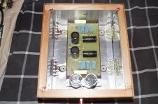
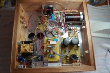
I built PCB with tubes, but now build them like this.
No stress on PCB.
No stress on PCB.
Attachments

Last edited:

Are you finding yourself in situations where you find the traces to be inadequate for the signal currents you are running? If not it's pretty immaterial if they do the job and don't degrade the circuit or safety margins.
I don't think so, this one was for building a big rectifier and pi filter board for my bench for use with the variac as a variable breadboarding supply. I figured I'd just beef it up. And have an excuse to try out my new reflow air soldering blower. 😉 Blew it with over 600F air and coated that whole trace in 15 seconds using just the regular roll of Kester leaded solder I always use.
With due respect, you are missing the point.OK respectfully I'm not asking about any of these things. All I'm doing is computing the cross sectional area of the typical PCB trace of 2mm wide by 1oz copper. And compared that number to the cross sectional area of the nearest wire gauge from the chart. And I came up with that a 2mm wide by 1oz copper PCB trace is equivalent to a 29AWG cross sectional area! Then I said to myself whoa! You mean a 2mm wide trace on a PCB board would be the same as if I used a crappy piece of 29AWG wire to connect those same parts with point-to-point. We would have to go out to 3oz copper boards and wider traces just to get to the equivalent of 22AWG doing point-to-point.
We use way thicker tan needed wires not because they are actually needed (duh) because of current passing through them, but just because of assembly convenience.
Imagine a wire connecting an input jack to a grid, with a 1M resistor to ground.
Hair thin is still too thick, it only needs a few copper atoms across.
Can you assemble an amp with such a wire?
No way!!!
You will use a gauge you can touch, strip and solder ... but don´t convert it to track width because that´s not the point.
Are you finding yourself in situations where you find the traces to be inadequate for the signal currents you are running? If not it's pretty immaterial if they do the job and don't degrade the circuit or safety margins.
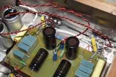
Here is the board bottom view, its a big pi filter of DC links, can use resistors or chokes. The hole is for a panel mount octal socket so I can either use a tube rectifier, or plug in a solid state rectifier substitute. The traces that connect the capacitors I coated with solder. Its my bench power supply in combo with a variac and isolation transformer 0-n voltage @ 200ma or more d2pending on what chokes I attach. I just wanted to beef up the capacitor traces. And I'm really sold on using panel mount tube sockets on standoffs over a hole technique, instead of using PCB tube sockets. The other traces are for bleeder, heater elev divider, snubbers ahead of the diodes and secondary fuses. The whole top side is uninterrupted copper ground plane.
Last edited:
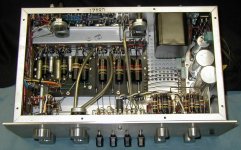
It's been done. This in the Marantz 7C, with turret board of course.And I'm really sold on using panel mount tube sockets on standoffs over a hole technique, instead of using PCB tube sockets.
Attachments
? We did that all the time in the bad old days of self-etched PCBs. That's why Steinmetz invented ScotchBrite.it would be hard to coat bare copper directly sticky-wise
Before ScotchBrite we polished just etched PCBs shiny copper bright and wiped them with "clock silver polish" fluid, which we bought at clock repair/jewellry shops.
Now I shiver thinking about the nasty poisonous chemicals it certainly had, but it deposited a nice even silver layer.
Unless it was mercury 😱
In theory, "liquid silver": 😱

Now I shiver thinking about the nasty poisonous chemicals it certainly had, but it deposited a nice even silver layer.
Unless it was mercury 😱
In theory, "liquid silver": 😱
I'd like to see George Anderson, aka Tubelab chime in. I pretty much copy what he seems to be doing with PCB sockets directly on the boards. I do mostly low wattage amps of 10W or less and always double sided with holes plated through and 1oz standard clad. No issue to date.
I recommend taking a look at the Saturn PCB Toolkit. It's a great calculator for trace spacing (high voltage compliance) and trace width (current carrying capability). Who cares what wire gauge a given trace is equivalent to as long as it can handle the current? Currents in tube circuits tend to be pretty small, except for the heaters.
I have no issue with board-mounted tube sockets. Use over-sized pads to prevent the socket from tearing out when you swap tubes. And beef up those heater traces (especially on output tubes).
Tom
I have no issue with board-mounted tube sockets. Use over-sized pads to prevent the socket from tearing out when you swap tubes. And beef up those heater traces (especially on output tubes).
Tom
Unless dc heater, why would anyone want to spred the ac heatercurrent strayfield with side by side thin and wide conductors? In regard to hum, this is about the worst someone can do! Use thin isolated, thigth twistet wires (magnet wire) to convine electromagnetic strays to a minimum, instead of spreading it out to the max.I have no issue with board-mounted tube sockets. Use over-sized pads to prevent the socket from tearing out when you swap tubes. And beef up those heater traces (especially on output tubes).
Tom
Last edited:
One little thing about using a chassis mount socket placed over a large hole in the PCB is that you can rewire the socket for an entirely different tube base. Use oval holes and you could even jump from octal to 9 pin tube without having to make a different PC board for either. Not that this would matter to anyone except a diy'er I know, but if you wanted to try your board with a 6sn7 then 30 minutes later use a 6cg7, just clip the wires and bolt on the other socket.
For point to point, thin professional audio cable works well as heater wiring: twisted to cancel the magnetic fields and shielded to shield electric fields.
On a PCB, you can use an ABA style layout: one wide F1 trace in the middle and two half as wide F2 traces on its sides. The magnetic fields of the two loops then also sort of cancel. In case of a multilayer board, you can also make an electric shield with a ground layer.
On a PCB, you can use an ABA style layout: one wide F1 trace in the middle and two half as wide F2 traces on its sides. The magnetic fields of the two loops then also sort of cancel. In case of a multilayer board, you can also make an electric shield with a ground layer.
All above are good points. If there is a choice between a 12V and 6V heater, use 12V, especially if, for some reason, you are forced to put the heater on a PCB. The thereby increased elctric field is seldom a problem and is easely shadowed by the advantages of the decreased track width and magnetic field.
I've never had any issues with traces on PCB with tube stuff and the VAPIDR board uses up to 700V. I mount tube sockets the the PCB, again no issues because I design the mount points so the board won't flex.
The output boards have 5 mounting holes, one in each corner and one in the middle between the tubes (which are 1.5" apart). There is no flexing, and no problems with heat even though I don't ventilate my chassis (looks ugly, I just design for high temperature operation instead)
I generally use 12V for heater circuits and place 6V tubes in series pairs.
I generally use 1mm traces for power, 0.5mm for signal, and 1.5mm for small tube heaters, 2.5mm or 3mm for 6P45S. Digikey's calculator says don't need to make the traces that big, either (based on a 3 inch long trace).
I've seen that. It is real Silver. And maybe Cyanide? I recall it got hard to get? Or we switched to a Tin-base solution? On the US market in the 21st century I find something similar, Silver, called "non-toxic"."clock silver polish"
Makes a lot of sense if you etch a pile of boards on Wednesday and can't get around to soldering until a week from Friday. Mail-order kits were always "tinned" so they did not go green in storage.
Me, I hotted-up the iron while I was rinsing the PCB. A few minutes on the hot-air vent and I could solder-coat a large board in a few minutes.
I fear some cyanide too, simply because it is so "good" in plating solutions.
That it kills the operator is just a little collateral damage 😈
You know I try to do as much as possib le in-house, so ponce I tfied it too.
I plate lots of things, such as metal corner protectors, skid feet, ruibbr leg caps, strip handle ends, etc. but my BIG expense comes from speaker frames and magnet plates, plating is charged by the kilo, withh 100 kilos being a "minimum lot".
I setup a "static bath", the simplest of them, where parts hang by wires from an electrode bar; submerged in a nasty solution which is boughtv ready made, and the other electrode is a brick sized zinc ingot.
It gets dissolved in the bath while floating zinc attaches to speaker frames.
So far so good, it did work, some problems at the beginning such as dull surface (there is a brightening bath for that), poor adhesion (metal must be perfectly clean), ugly scales and "bubbles" (too much current), etc. but all that is normal and expected, teething troubles, practice makes perfect.
But when I asked my supplier he said: "no big deal, boil the frames first in this solution" ..... which did REALLY clean them.
What was it made of? .... basically cyanide.
When I complained: "hey, all your baths contain at least a little cyanide" 😱
I slowly disassembled everything and got rid of chemicals, that is ONE operation I am happy to pay and wait for "outside".
I tried nickel plating, but nickel sulfate is almost as nasty, so ....
- Home
- Amplifiers
- Tubes / Valves
- Are PCBs too wimpy for tubes? (compared to wire cross sectional area)