I thought I am going to give an update here on current progress of the digital version of Bob's THD Analyzer. I finished bench-testing for all 3 PCBs, these bench-tests had to be rewritten, since we now use the microcontroller to switch input-levels, sensitivity and frequency. And I had to add tests for all the relays, to make sure they switch properly.
I made a couple of iterations for the uC PCB, the ADC channels suffered from the switching-spikes of the seven-segment displays (TM1637), so we created a new PCB for these seven-segment displays (SSD). We, because I now work together with a nice gentleman from Sweden, who created the power-supply boards and these TM1637 PCBs. Every SSD now has a maximum of 3 LEDs next to it (also switched by the TM1637), for amplitude readings we can set Vpp, Vpeak and Vrms. For sensitivity we can switch between % and dB, with the lowest % readings expressed in ppm. Settings can be entered with up/down/left/right/ok keys and are stored in eeprom. The LCD display (20x4) shows all analyzer settings, while the SSDs show actual readings. I also stored calibration settings in eeprom, and these can be changed to further improve accuracy. These calibration settings are basically the full-scale values for the ADCs: for each sensitivity- and input-level there's a separate full-scale value. The readings of output-level, input-level, distortion and frequency now work fine, which is a good base for further system-level testing.
I am trying to update the github repository as good as possible with all design files and software changes, but up until now, we used Bob's original articles a lot. I made 31 commits so far and the latest firmware revision is V0.23.
Anyway, progress is good, it will probably cost me another year or so to iron out all bugs and finish calibration and system-level testing, which is the next thing to do.
Just a question left for you guys: the function-generator PCB works fine up until 130 kHz. I am using lots of SMD components and vias on this board which might impact performance and therefore was considering an update to this board. Since each via also introduces some inductance and Bob's original boards went all the way up to 200 kHz, I am thinking of a redesign here. Maybe go back to through-hole components for the analog part? Maybe a 4-layer board? Any thoughts on this? Would it be worth the trouble?
Intriguing that Bob’s hand wired/point to point wiring, remote switches etc. outperforms your smt version of the same design.
I need to look at your implementation before I can offer any advise as to possibilities.
I need to look at your implementation before I can offer any advise as to possibilities.
Yes, it is indeed intriguing! I experimented with lots of things, first had chinese NE5534s (my bad), then replaced them by LM4562s and OPA1612s, then replaced them again with original NE5534s. I moved the 20-200 kHz caps closer to the opamps and used the exact same type of caps Bob specified. With the chinese stuff I could only get to 2 kHz, with the real opamps that was way better (100-130 kHz). There was not much difference between LM4562s, OPA1612 and the real NE5534s. Also the change of placement of CKM4 and CLN4 (220 pF, mica) did not do much. I also changed the values of RKM4 and RLN4 (the series resistors for CKM4 and CLN4) to 330 Ω (from 68 Ω), experimented a lot with them and higher values definitely improved the situation. Maybe Bob's added cable capacitances would improve performance in some way? Or my use of via adds too much inductance? Resistors used are typically SMD1206 thick film resistors.
The board itself is a 2-layer board with top and bottom ground planes. All the design files are located here: https://github.com/Emile666/THD_Analyzer. There's also a link to the PCB1 design files, it includes the Eagle source-files as well. Sorry for not having Kicad files yet, I still have to change one-day, but creating a board in Eagle for me is just so much more convenient than in Kicad.
Thanks for any help!

That's fine I do not use Kicad either. Lots of hard work to get it this far, cheers to you.
I took a quick look at the gerber "pcb1_relay_v030_combined_2024-07-10.zip"
I've never had GerbTool bark so much, reading in those gerbers, but it looks to be loaded okay, drills too 🙂
wow 6 mil trace-trace spacing. I need to spend more time looking at the layout and follow along with your schematics to comment further.
I had indeed set DRC to 6 mils and JLCPCB didn't have any problems creating it, quality of the boards produced was very good. The digital part is at the bottom and the analog part (Bob's) is located at the top. I needed to connect a number of signals (mostly the E signals) from the relay outputs to the analog parts, thus creating long traces with vias. Maybe that's part of the problem. Other than that, the digital and analog parts are separated as much as possible. Most signals are named in Eagle, so you can follow them through.
Okay, I've looked at the layout enough to provide a few comments.
Imo it's not advised to use parallel footprints, IC1 || IC12A, IC2||IC12B etc. layout for the NE5534A as was done originally (single), sub OPA1655 or other single packaged devices, as necessary. that will clean up the layout considerably. I would not use any leaded parts, mica caps etc, use MLCC NPO(COG) instead. leaded ecaps are fine to use.
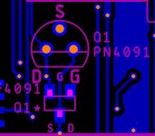
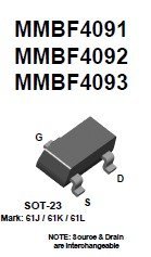
You have a no connection to Q1* (SOT-23) source, sch shows it in || with Q1, source is not connected to ground, a DRC error in the copper pour, oops
Imo it's not advised to use parallel footprints, IC1 || IC12A, IC2||IC12B etc. layout for the NE5534A as was done originally (single), sub OPA1655 or other single packaged devices, as necessary. that will clean up the layout considerably. I would not use any leaded parts, mica caps etc, use MLCC NPO(COG) instead. leaded ecaps are fine to use.
You have a no connection to Q1* (SOT-23) source, sch shows it in || with Q1, source is not connected to ground, a DRC error in the copper pour, oops
Attachments
Last edited:
Thanks very much for your comments! I will definitely remove all the parallel components in a future revision. Interesting observation about the leaded parts, I think component choice is even more critical than I thought. I will update the BOM with MLCC NPO(COG) components!
The Q1*-source is connected via GND, I checked the gerber file myself and it seems fine. Also, the board itself shows a connection, so no worries here. Thanks again for helping!

The Q1*-source is connected via GND, I checked the gerber file myself and it seems fine. Also, the board itself shows a connection, so no worries here. Thanks again for helping!
Version 3 of my Tutorial for the QuantAsylum QA403 audio analyzer is now up on my website and is discussed in the QuantAsylum User Forum. The tutorial walks the reader through all of the pertinent tests for an audio power amplifier, in this case my BC-1 design, which is also described in detail on my website.
The QA403 is an outstanding piece of equipment, especially at only $600. It has pretty much all of the functionality and performance most people could need. It is just as valuable for use with small-signal circuits as well as power amplifiers. One nice feature is that it includes selectable inverse RIAA respnse shaping for measuring phono preamps. It also includes selectable A-weighting for noise measurements. Further, it includes optional user-entered weighting responses. It can usually see distortion products below -120 dB or better, and report THD down to -120 dB or better. It can sample at up to 192 kHz, allowing one to see FFT products up to at least 80 kHz. Sampling to 384 kHz may be available soon. It is powered from its USB connection to the PC on which its software resides, and it is galvanically isolated from the PC side. It has balanced I/O.
Cheers,
Bob
I am very excited to see an active discussion about this analyzer. Having started my build in the fall of 2022 I am very near completion. It’s amazing how the modifications I made are the same ones others have mentioned (input attenuator compensation, true RMS metering, etc). @Emile666 your build is very impressive and I feel you on the frustration with the higher oscillator bands. I had a lot of battles with my oscillator and I had to do a lot of parts swapping to get it working good. My build is through hole so much easier to do than smt. I’d be happy to offer any help from my learnings.
Its great to hear about all this progress and excitement about the analyzer. I remember when I first built it a long time ago that I had relatively little trouble getting it to work well in spite of the large amount of labor in wiring up all of those crude multi-gang switches. The idea of replacing them with relays and using a microcontroller really makes sense. However, there were two things that I seem to recall that required some extra work to get right. Back then I was less informed about capacitor choices and learned that one or two of the capacitors for frequency band selection needed to be changed to get good performance and stability. I don't remember which ones they were, but using today's high-quality capacitors, like polypropylene and and the like should cure that problem. I did have to do some tweaking on the highest frequency band of 20 kHz to 200 kHz due to some extra phase lag in the op amps at the higher frequencies. The main solution for that was to put a bit of resistance in series with the high-band capacitors in the integrators.
Cheers,
Bob
Cheers,
Bob
I will check mine when this weekend, but I think I also tweaked the values of the series resistors on the 200K band. I used polystyrene capacitors for the 200K band. I used WIMA film caps for the others. My build uses the rotary switches like the original design. I was able to find lots of Centra lab parts between eBay and ham fests, and I have quite a stockpile now of switch parts. I used quite a smattering of different op-amps in the oscillator (LT1468s, OPA604, LM4562) as well as 5534/318 in some positions. My bench includes a most exellent HP3585B which between it and a tuneable notch filter have allowed me to make very low harmonic measurements.
Measuring its own distortion, my CDA measures 2K/3Vrms at 0.0003% (-110dB) and 200K/1Vrms at ~0.0063% (-84dB). These are rms values as I've emplemented true RMS measurement using the AD536. The 2Khz value is limited by the CDA's null as the fundamental level is higher than the harmonics.
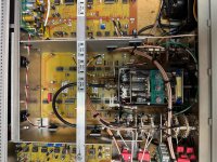
One problem I've noticed is that at the extreme high end (200Khz), the instrument is only stable at the nominal 0dB input level. If i try to measure 200Khz 3V on the 3V range (which the instrument should be capable of due to the auto-set level) my instrument becomes unstable. I can measure it fine however if I range up to the 10V range (which puts the input level back at the 0dB level). This problem does not occur on the lower bands even as high as 160Khz. I'd be interested to know if anyone has experienced this. I've also included a photo (partial) of my build for information.
Measuring its own distortion, my CDA measures 2K/3Vrms at 0.0003% (-110dB) and 200K/1Vrms at ~0.0063% (-84dB). These are rms values as I've emplemented true RMS measurement using the AD536. The 2Khz value is limited by the CDA's null as the fundamental level is higher than the harmonics.
One problem I've noticed is that at the extreme high end (200Khz), the instrument is only stable at the nominal 0dB input level. If i try to measure 200Khz 3V on the 3V range (which the instrument should be capable of due to the auto-set level) my instrument becomes unstable. I can measure it fine however if I range up to the 10V range (which puts the input level back at the 0dB level). This problem does not occur on the lower bands even as high as 160Khz. I'd be interested to know if anyone has experienced this. I've also included a photo (partial) of my build for information.
Attachments
Last edited:
VERY nice implementation in that great picture. Much cleaner than mine! I like the shielding of compartments. I'm impressed that you were able to find all of the parts for making those big rotary switches. Quite a few years ago I also upgraded mine, also using the AD536.
I'll put mine in loop back and see if I can duplicate the high-band behavior you described.
Cheers,
Bob
I'll put mine in loop back and see if I can duplicate the high-band behavior you described.
Cheers,
Bob
I look forward to what you find out. I've made some changes to the oscillator based on readings from this forum and the works of the late Dick Moore on his archive site Tronola. Most significant of which is the 2nd harmonic trim around the level control FET. I'm in the process of putting together a file of my build which includes a lot of photos and details of the modifications and changes I implemented. Once it's finished, I would be happy to post it hear for those who might be interested.
As I finish my distortion analyzer build and doing more testing I've come across an issue in the product filters. I built the tracking filters which added greatly to the switching complexity. When I feed the analyzer with a known distortion value signal, the reading is low on the my analyzer. This issue occurs at the bottom of the band (for example at 20Hz on the 200 band). The measured distortion value is about -2.6dB low. So, If I apply a known distortion value signal of 10%, my analyzer reads 7.5% (2.6dB low), while my "reference" analyzer, an HP339A will show the correct value of 10%. This error becomes smaller as I make the same measurement on successively higher frequencies in the band, and by about 100 Hz the error is only -0.3dB. At the top of the band, the error is gone.
I've isolated the problem to the product filters. If I bypass the filters, the error goes away. The distortion signal coming into the filters is a correct value. 300mV at E29 gives me full scale indication, which I should have for a 10% distortion test signal. This problem is identical on the 200, 2K and 20K ranges and the behavior is identical. The error starts at about -2.6dB low and becomes less and less as the test is progressed through the band. The error seems shared by both filters. The LPF contributes 1.3dB and the HPF contributes the other 1.3dB. Observed by bypassing the filters one at a time.
So I did some testing on the breadboard, building the filters and testing their response. The breadboarded filters behaved in the same way. Here is what I found. On the low pass filter, if I remove R171 the error goes away. This is the 100K resistor between the non-inverting input of the buffer and ground. I've replaced it with a 1M resistor and the error is only -0.3dB at the bottom of the band. I can live with this error if I must, but I'd like to remove it all together.
I've checked my switches and wiring, everything is correct so I know this issue is not because I've got tuning components out of order. A lot of filter schematics I've seen don't include this resistor and I'm wondering if it can be omitted. I'd like to know if anyone else has experienced this or knows of a better fix. I'm not looking for circuit diagnosis, just any thoughts. Thanks!
FWIW I have replaced R171 and 174 with 1M resistors. Spot checks of the 200, 2K and 20K bands show a much better accuracy. Measurements are now within 0.1dB of my reference analyzer and spectrum analyzer. I'll have to do more rigorous testing but this looks promising.
Watch the DC levels at the outputs of the LM318 op amps. Those are earlier bipolar input types and the 100K was probably selected due to input bias currents.
A quick check of DC levels shows about 8mV at the output of IC32 and 3mV at the output of IC33. In loopback I can see no change in my residuals from before and after. Also my monitor buffer and true RMS converter are capacitor coupled so any DC level there will be blocked.
The above checks have been made after I swapped the LM318s for AD797s in the filters as I had them before. These are probably overkill but the noise level is slightly lower with the low noise OPs. I had originally observed my problem while using the 797s and it persisted after swapping back to the 318s.
The above checks have been made after I swapped the LM318s for AD797s in the filters as I had them before. These are probably overkill but the noise level is slightly lower with the low noise OPs. I had originally observed my problem while using the 797s and it persisted after swapping back to the 318s.
I'm sorry I've taken so long to get back on this issue. I think you got it right and did the right thing. When I did the design, I did not adequately take into account the amount of attenuation at the low end of the band where the switched frequency determining resistors get to be a larger value, leading to a voltage divider effect where the 100-k resistor is the shunt leg. I'm sure I was worrying too much about DC offset due to the input bias current of the bipolar op amp. Nowadays, I would use a JFET op amp with adequate bandwidth and decently low noise. Thanks again for pointing this out.
Cheers,
Bob
Cheers,
Bob
- Home
- Design & Build
- Equipment & Tools
- Another realization of Bob Cordell's THD Analyzer