10 turns probably isn't enough, I've been through this thinking something is wrong when I just needed to keep turning.
Hmmm... I agree with McQuade, keep turning. That fact that you have zero offset at the moment is (kinda) good.
The other thing I'd check is to make sure that the ZTX450 and 550 are in the right spots. They appear to be facing the proper way, but make sure the devices themselves are not transposed.
The other thing I'd check is to make sure that the ZTX450 and 550 are in the right spots. They appear to be facing the proper way, but make sure the devices themselves are not transposed.
So you don't have enough voltage to turn on the mosfets. 🙁
And this is after you've turned P1 and P2 a number of times? What
resistances are you seeing across R5 and R6?
What resistances/voltages do you see across R3 and R4?
Just stopped by for lunch and thought I'd check the resistances on the right channel that I have dialed in (I believe - see above) to compare with the left I am trying to get going. F6 is .648k and F5 is 1.612K. Seems to be quite the difference no?
Not really. There are three things working in concert to get the bias set, per side, and as there’s almost always a volt difference in Vgs between the N and P channel mosfet, id actually say it’s normal, and having equal resistances would be very very rare.
Hello and my apologies for being away without finishing up here - summer got in the way.
I spent a couple of hours this afternoon going over where I left off: I powered up and checked the Right channel: R7 is .598dcv, R8 is .592dcv and the speaker terminal is .01dcv.
I zeroed out the pots again for the left channel (down to .2 ohm) and started over but as before, there is never any change at R7, 8, or the terminals. Dennis mentions I need 3.5v across R5 and 6 to get anything through to 7 or 8 but I get no voltages across 5 or 6 either, doesn't matter what I do with the pots.
I have a corresponding 22.69v at the V- & V+ on both channel boards.
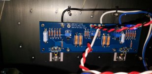
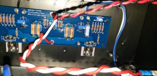
Q5 & 6 are installed correctly as are Q1 & 2.
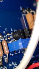
Troubleshooting suggestions in basic plumber english would be appreciated.
Dave
I spent a couple of hours this afternoon going over where I left off: I powered up and checked the Right channel: R7 is .598dcv, R8 is .592dcv and the speaker terminal is .01dcv.
I zeroed out the pots again for the left channel (down to .2 ohm) and started over but as before, there is never any change at R7, 8, or the terminals. Dennis mentions I need 3.5v across R5 and 6 to get anything through to 7 or 8 but I get no voltages across 5 or 6 either, doesn't matter what I do with the pots.
I have a corresponding 22.69v at the V- & V+ on both channel boards.
Q5 & 6 are installed correctly as are Q1 & 2.


Troubleshooting suggestions in basic plumber english would be appreciated.
Dave
Last edited:
I spent a couple of hours this afternoon going over where I left off: I powered up and checked the Right channel: R7 is .598dcv, R8 is .592dcv and the speaker terminal is .01dcv.
?? That's basically perfect.
What's the amp not doing?
The Left Channel is not getting those results. No matter what I do with the pots, I get no change whatsoever at R7 or 8 nor at the speaker terminal. If I had started with this channel I might be thinking I'm measuring incorrectly but as you said, The Right channel came out pretty much perfect so I know I'm setting the pots to zero(ish) and which way to turn them correctly as well as checking voltages properly.
Hi Dave,
Seems like you right channel is fine but you still have problem with the left.
With the left channel, what voltages do you measure across R3 and R4?
Dennis
Seems like you right channel is fine but you still have problem with the left.
With the left channel, what voltages do you measure across R3 and R4?
Dennis
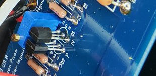
Try reflowing the JFET solder junctions. All of them should look like the D pin on your K170 (with the solder wicking up the pin). The S and G pins look a bit dodgy.
Try reflowing the JFET solder junctions. All of them should look like the D pin on your K170 (with the solder wicking up the pin). The S and G pins look a bit dodgy.
Hey Jeff. Okeedoee. I'll have to pull that side of the case off then. Back in a bit. Thx.
Check the resistance between the Source pin of the 2SJ74 and the ground on your power supply board.
Do the same between the Source pin of the 2SK170 and the ground on your PSU board.
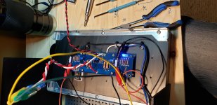
Your second picture shows you measuring the voltage across R5 and R6. Are those zero? If so, are both sides of R5 24V, and both sides of R6 -24V?
Do the same between the Source pin of the 2SK170 and the ground on your PSU board.
Your second picture shows you measuring the voltage across R5 and R6. Are those zero? If so, are both sides of R5 24V, and both sides of R6 -24V?
Can I assume the S leg is the Source pin? I have 15.2 ohms on the K170 & 9.0 ohms on the J74
And I am measuring voltages across R7 & 8 - they are zero. R7 is 22.7V off both sides and R8 is -22.7 off both sides.
And I am measuring voltages across R7 & 8 - they are zero. R7 is 22.7V off both sides and R8 is -22.7 off both sides.
Yep, S is Source. The resistance values look fine. (While you're at it you might want to trim P3 so that those two readings are the same, but that's not your problem.)
What's the voltage on the G pins of the two JFETs?
What's the voltage on the G pins of the two JFETs?
OK, one more test. Do you see 22.7V and -22.7V on the D pins of the JFETs?
Indeed I do.
- Home
- Amplifiers
- Pass Labs
- Another F5 Build
