Yes.
So in the Ohmic region any ripple on the power supply will show up on the output of the source pin. In the pentode region this ripple has no effect on the output of the source pin.
So in the Ohmic region any ripple on the power supply will show up on the output of the source pin. In the pentode region this ripple has no effect on the output of the source pin.
Thanks Pico.I guess that is why everyone running the B1s in saturation region. The temperature drifts as mentioned by Dennis Feucht is possible at Saturation region, but the effect is an offset voltage that will be blocked by DC blocking capacitor?
But PSRR is more desirable quality to look for?
But PSRR is more desirable quality to look for?
In my opinion the issue of the thermal drift is overstated in many cases.
Once you add some source resistance the effect is reduced even further.
In your case you are using an output cap you can just ignore it.
You certainly don't want noise, so good psrr is always a good thing.
Once you add some source resistance the effect is reduced even further.
In your case you are using an output cap you can just ignore it.
You certainly don't want noise, so good psrr is always a good thing.
Last edited:
I think it is the opposite. It is because the B1 uses the two devices with Id = Idss that thermal drift drops out of the equation.
It goes back to my explanation earlier. If you operate both devices at the same current and at the same voltage, then they both dissipate the same power and thus run at the same temperature.
It goes back to my explanation earlier. If you operate both devices at the same current and at the same voltage, then they both dissipate the same power and thus run at the same temperature.
Was wondering where were you!!
Andrew, so if you run devices near their IDss they are going to run hot but they may get heated to the same level as same current pass through them and they also develop same voltage across drain and source, did I understand correct?
Also the issue with temperature drift is there might be an offset voltage between input and output. But B1 using a capacitor at output anyway to block it. It seems like recommendation is to run the devices with ID at 75-80% of IDss
Other than may be keeping the devices cooler, what is the advantage of adding a source resistor ?
Initially I was thinking to run the devices in ohmic region , but as Pico mentioned the PSRR will be better if they run near saturation for buffer amp .
I read it after, in other documents too without stating actual reason to Keep ID near IDss.
Last edited:
The beauty of the B1 ia that it uses closely selected Idss jFETs and maintains good temperature matching that any Member can obtain with simple test instruments. It works.
When you reduce the current using source resistors you move to a different part of the curves for the two devices. Now you will find that the two similar Idss devices do not match. They have different gm, even though the Idss could be identical.
If you choose to operate two selected jFETs at a lower current, then you should be matching gm AND Idss. That is a very different set of test and measurements.
The easy way is not to bother matching (different from selecting Idss) and just accept the performance that results.
Have you read E.Borbely?
He has published many papers, all are worth reading. In there you will find a recommendation to use a Vds that is at least twice Vpinch-off. This rule applies to all jFETs used for many different purposes.
Last edited:
I think you may be right.
I did not test for that when matching devices, since the devices never have to operate at 100nA
I went down to 20% or 25% of Idss.
I did not test for that when matching devices, since the devices never have to operate at 100nA
I went down to 20% or 25% of Idss.
Andrew ,20-25% of Idss put the devices at ohmic region. Pico points out this region ID would have a linear relation with VD and hence will make it susceptible to supply voltage issues. Within my limited understanding it seems right to me. Almost all the article I read about Jfet also states for usual amplifier applications Jfet is used in saturation region.
Regular B1 design uses full Idss. But Feucht paper says most significant noise from these devices are thermal distortion.for me the devices running at Idss should have more thermal noise?
While Feucht paper is focusing on avoiding voltage offset by running 0.8V higher than pinch-off voltage ( means closer to Vgs=0).
Does this means picking a smaller Idss device 2sk170 will have best result as the heat generated is lowest?
Last edited:
Also matching with IDss will be less than ideal option in picking Jfets.
I experimented myself with different source resistors and seems like it is true.
IDss matched JFet may not behave same at a different ID.
Lab 4 - JFET Circuits I | Instrumentation LAB
Please read problem 4:15.
In my less than sophisticated measurement it seems the one matched at IDss will have different ID at ohmic and saturation region.
So the inference is if moving away from IDss ( B1 design) using resistors
1. Decide where one want to operate the JFet, ohmic versus saturation.
2. Then pick the Rs value (Vgs/ ID) or closer and match the devices.
3. if possible match them for Vp
I bought 25 BF862 and has 2 perfect matches and more than 3,1% matches.
not if you follow Borbely's advice and ensure that Vds >2*Vpinch-offAndrew ,20-25% of Idss put the devices at ohmic region.
the B1 uses a Vds ~ 15*Vpinch-offPico points out this region ID would have a linear relation with VD and hence will make it susceptible to supply voltage issues. Within my limited understanding it seems right to me. Almost all the article I read about Jfet also states for usual amplifier applications Jfet is used in saturation region.
Regular B1 design uses full Idss.
I think you have mis-interpretted what D.Feucht was suggesting.But Feucht paper says most significant noise from these devices are thermal distortion.for me the devices running at Idss should have more thermal noise?
While Feucht paper is focusing on avoiding voltage offset by running 0.8V higher than pinch-off voltage ( means closer to Vgs=0).
Match the Rs and match the devices and both Vgs will be equall and thus the output offset becomes zero
No, the Pq depends on Id*VdsDoes this means picking a smaller Idss device 2sk170 will have best result as the heat generated is lowest?
It's the combination of both voltage and current that determines the device dissipation and thus device Tj.
I have been pointing this out for nearly a decade. There are many who select jFETs by Idss and refer to them as "matched". They are not matched they are merely selected for near equal Idss......................
IDss matched JFet may not behave same at a different ID.
I think you are still mixing up the two operating regions.Lab 4 - JFET Circuits I | Instrumentation LAB
Please read problem 4:15.
In my less than sophisticated measurement it seems the one matched at IDss will have different ID at ohmic and saturation region.
So the inference is if moving away from IDss ( B1 design) using resistors
1. Decide where one want to operate the JFet, ohmic versus saturation.
2. Then pick the Rs value (Vgs/ ID) or closer and match the devices.
3. if possible match them for Vp
I bought 600 LSKs and got lots of Idss matches to better than 0.1%I bought 25 BF862 and has 2 perfect matches and more than 3,1% matches.
But that is simply batching them by selecteing Idss.
Then comes the measuring exercise to find matches that track each other as Vgs is altered.
Idss is cheap and quick. I found that obtaining matched pairs took at least 10 times longer. If memory did not play tricks, I might claim it took 50 times longer.
Andrew , sorry but something I can't grasp is how the VDS affect IDss.Yes it does change ID but once VDS meets or exceed the 2 times V-Pinch off ,current plateau and then until IDss it stays in saturation region.
So regardless how much more VDS one applies 25% of IDss , so for example mine are mostly in 15ma IDss BF862s, 25% of which is close 3.5ma. It only falls at Ohmic region of IDss -VDS plot.
So at more than 2 V pinch off the current can not be 25% of IDss.
What I understand is for a given Vgs, ID can not be 25% of IDSs once VDS exceeds V pinch off. It will be at least 75% of IDss .
Last edited:
Vds could be 7Vds
Id could be 4mA
Dissipation will be 28mW
Now look up the Id vs Vgs plot in the datsheet and you'll find the required Vgs for each of the typical devices shown in the graph.
The 4.1mA idss version will need a Vgs of ~0.005Vgs
The 6.2mA will need ~0.095Vgs
The 8mA will need ~0.145Vgs
The 10mA will need ~0.2Vgs
I think you need to go back and re-read Borbely and Feucht and learn how to interpret a datasheet.
Last edited:
Andrew ,is it Bf862 data sheet? Is it possible to draw them out if you have some time.
I will do it tomorrow perhaps and see if I am making any sense.
I will do it tomorrow perhaps and see if I am making any sense.
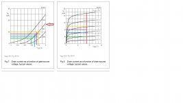
Since you have plotted values on one curve I'll use the same curve for this example.
The middle curve shows Id ~17mA when Vgs=0V
When the Vgs is increased to -0.2V the current has reduced to 10mA
If we go up to -0.4Vgs, the current is now ~4mA
That tells you that for a 17mA Idss device you need to apply ~ 0.4Vgs to the device to set up a 4mA bias current.
Now look at the right hand plot and see if that confirms what I have just read off the Id vs Vgs graph.
We know that the Idss is measured when Vds is at 10V.
Look at the bottom and find 10Vds.
Go up till you reach the -0.4Vgs curve. Now read off the Id. Could be ~ 4.3mA
Pretty close.
Now go and measure your device at 4mA (Pq= 40mW, it will get slightly warm so results will not be identical to the datasheet). What Vgs do you need to apply to get that 4mA?
Now reduce the Vds to 7V, just to compare to the hypothetical example I started with yesterday. What Vgs is required to get 4mA when Vds = 7V?
Andrew,
I am not understanding why you are asking about a different VDS at a given VGS.
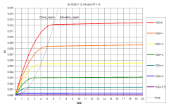
ID = IDSS * [1 - (VGS/VP)]2
ID has no relationship with VDS.
At saturation region IDS is not affected by VDS. It can be a VDS of 8V or 10 V or 12 V, IDs is only related to VGS.
So to answer your questionat 7v VDS it still need a VGS of -0.4V if you want to have an IDS of 4ma.
Since the IDS has a slope in real JFETs, there might be small changes in Vgs needed but it is still the same VGS.
Going back to my previous inference that ID you suggested is still in ohmic region of VI curve.Then yes VDS will affect the ID.
this is from page 30 of Borbely's article that is attached here.
The Transconductance Curve
As mentioned previously, you can use the JFET as an amplifier in the pentode, or
saturation, region. Here the VDS has little
effect on the output characteristics, and
the gate voltage controls the channel current ID
I am not understanding why you are asking about a different VDS at a given VGS.
ID = IDSS * [1 - (VGS/VP)]2
ID has no relationship with VDS.
At saturation region IDS is not affected by VDS. It can be a VDS of 8V or 10 V or 12 V, IDs is only related to VGS.
So to answer your questionat 7v VDS it still need a VGS of -0.4V if you want to have an IDS of 4ma.
Since the IDS has a slope in real JFETs, there might be small changes in Vgs needed but it is still the same VGS.
Going back to my previous inference that ID you suggested is still in ohmic region of VI curve.Then yes VDS will affect the ID.
this is from page 30 of Borbely's article that is attached here.
The Transconductance Curve
As mentioned previously, you can use the JFET as an amplifier in the pentode, or
saturation, region. Here the VDS has little
effect on the output characteristics, and
the gate voltage controls the channel current ID
Attachments
Look at the slope on those curves. It small but detectable.
Even you have stated:
Now look back at the BF862 data you posted, the slope is enormous by comparison.
Borbely tells us
The slope on the jFETs is similar to Early voltage in a BJT.
Even you have stated:
Since the IDS has a slope in real JFETs,
Now look back at the BF862 data you posted, the slope is enormous by comparison.
Borbely tells us
Don't you believe?As mentioned previously, you can use the JFET as an amplifier in the pentode, or
saturation, region. Here the VDS has little
effect on the output characteristics, and
the gate voltage controls the channel current ID
The slope on the jFETs is similar to Early voltage in a BJT.
- Status
- Not open for further replies.
- Home
- Amplifiers
- Pass Labs
- Another B1 design