How Andrew Russel came with resistor value 49 ohm where Patrick is using much higher current and lower Source resistors .
Is he operating the Jfet in ohmic region Where Jfet act as resistor vs saturation region where it is a current source?
Is he operating the Jfet in ohmic region Where Jfet act as resistor vs saturation region where it is a current source?
I still have not got the answer from anyone about how Andrew Russel came with resistor value 49 ohm. Is he operating the Jfet in ohmic region Where Jfet act as resistor vs saturation region where it is a current source?
Not worth trying to understand.
Not ohmic region.
He simply wanted to operate at lower current.
Please read page 8. I think there is a reason why he is selecting that lower current.
http://hifisonix.com/wordpress/wp-content/uploads/2015/01/UBx.pdf
"if we do not want to individually select the JFET’s (i.e. just order them and place them on the board with a guaranteed good result) we have to ensure that at the upper Id extreme (top curve in LHS panel), we do not exceed the Idss 10mA figure at 5V p"
Is this means if we keep Idss below 10 we can avoid matching.
Last edited:
1) The typical Idss figure of a bf862 devices is around 18mA.
2) The minimum Idss figure of a bf862 part is 10mA
3) He wants to achieve 5V peak into 10K load. This requires 5/10k = 0.5mA Id bare minimum (not sure how he come up with 2mA, possible mistake). Obviously running at greater than 0.5mA will be beneficial.
4) His target Id figure is 6.5mA which requires exactly 49.2 Ohms if using a typical Idss part. But they don't make 49.2 so going down to 47 Ohms is the most appropriate resistor.
5) If using a 10mA Idss part with 47 Ohms there will still be enough current to drive his load and if using 25mA part with 47Ohm it won't exceed power limits of device or exceed the Idss min of 10mA.
Basically the greater your source resistance the less variation you will have in Id betwee max and min Idss parts.
Cut it short, have to go to work now.
Ok, I think I am getting close to something .
From Dennis Feucht's article
First design feature of matched jfet is static DC tracking of matched transistors(JFETs). Which means zero offset voltage from input to out put.
This is what B1 native design do as explained by Fauchet.
If the gate of the lower Jfet, is connected to its source,then VGS=0V ,and the drain current will be IDss.Since the same current passes through upper Jfet and since it is matched its VGS=0 too and there is no DC offset. But when temperature changes this tracking can change. So he recommends to change operating point to zero Transfer Characteristic point of Jfet's transfer curve, where thermal drift of VGS is minimal for a given Id, for a given temperature.
For Jfets the Zero-drift VGS is about 0.8V above the pinch-off (Vp)Voltage. Feucht names that zero drift VGS as VGSZ.
It is also the point where ID traces at various temperature intersects in transfer characteristic plot. Please refer the article attached.
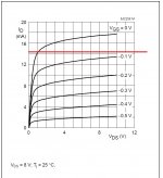
(Pinch off voltage is the drain to source voltage after which the drain to source current becomes almost constant and JFET enters into saturation region and is defined only when gate to source voltage is zero.)see the picture attached.
So for 2N5485 ID range of 4-10 ma,and Vp= -2V he selects 5 ma as ID So VGSZ= -2+0.8=-1.2V.
Rs is calculated as 1.2V/5ma=240 ohm.
This is my calculations for BF862. Please correct me if you find it wrong.
Unfortunately for BF862 transfer curve with ID at different temperature is not available in datasheet.
But V-I curve is available. Id range for BF862 is between 10-25ma. I would limit the current at 12ma.
From the ID -VDS plot ( See attached) Vp= 1V ,so VGSZ=1.8V
Source resistors for each Jfets 1.8V/12ma= 150 Ohm.
I think keeping Id close to ohmic region( before Vp) in V-I plot ,will have linear output characteristic when used as a audio buffer.
From Dennis Feucht's article
First design feature of matched jfet is static DC tracking of matched transistors(JFETs). Which means zero offset voltage from input to out put.
This is what B1 native design do as explained by Fauchet.
If the gate of the lower Jfet, is connected to its source,then VGS=0V ,and the drain current will be IDss.Since the same current passes through upper Jfet and since it is matched its VGS=0 too and there is no DC offset. But when temperature changes this tracking can change. So he recommends to change operating point to zero Transfer Characteristic point of Jfet's transfer curve, where thermal drift of VGS is minimal for a given Id, for a given temperature.
For Jfets the Zero-drift VGS is about 0.8V above the pinch-off (Vp)Voltage. Feucht names that zero drift VGS as VGSZ.
It is also the point where ID traces at various temperature intersects in transfer characteristic plot. Please refer the article attached.
(Pinch off voltage is the drain to source voltage after which the drain to source current becomes almost constant and JFET enters into saturation region and is defined only when gate to source voltage is zero.)see the picture attached.
So for 2N5485 ID range of 4-10 ma,and Vp= -2V he selects 5 ma as ID So VGSZ= -2+0.8=-1.2V.
Rs is calculated as 1.2V/5ma=240 ohm.
This is my calculations for BF862. Please correct me if you find it wrong.
Unfortunately for BF862 transfer curve with ID at different temperature is not available in datasheet.
But V-I curve is available. Id range for BF862 is between 10-25ma. I would limit the current at 12ma.
From the ID -VDS plot ( See attached) Vp= 1V ,so VGSZ=1.8V
Source resistors for each Jfets 1.8V/12ma= 150 Ohm.
I think keeping Id close to ohmic region( before Vp) in V-I plot ,will have linear output characteristic when used as a audio buffer.
Attachments

Last edited:
Absolutely of no interest.
I design stuff like a Formula 1 racing car not like a wheel chair designed for disabled people.
Vpinch-off is obviously important to take into consideration.
I will go through it and explain the best I can for you. I will print out the original article and read it properly, I hate reading off a computer screen.
Last edited:
Absolutely Pico. But keep in mind people who always go on F1 cars may ending up needing a wheelchair too 😉.
Please interpret the article that's all I did. I have no formal training in Electronics so I do not claim to be a designer. But I am a science person and if I can't understand why I lose sleep over it.
Please interpret the article that's all I did. I have no formal training in Electronics so I do not claim to be a designer. But I am a science person and if I can't understand why I lose sleep over it.
Absolutely Pico. But keep in mind people who always go on F1 cars may ending up needing a wheelchair too 😉.
Please interpret the article that's all I did. I have no formal training in Electronics so I do not claim to be a designer. But I am a science person and if I can't understand why I lose sleep over it.
That is why simple is better.
My approach is
1) Matching or characterising devices
2) What is the maximum current I can run though this sucker without destroying it.
Hahaha
Made bf862 spice models with Idss of 25mA and 10mA, to simulate worst case scenario.
Ran some simulations.
Fell asleep.
It's hard to be motivated to study an inferior design.
Ran some simulations.
Fell asleep.
It's hard to be motivated to study an inferior design.
I think keeping Id close to ohmic region( before Vp) in V-I plot ,will have linear output characteristic when used as a audio buffer.
Just having lunch.
Ohmic region is of no benefit for source follower buffer.
Please explain why? Actually what is the benefit in running at saturation region?
PSRR.
You're not looking for voltage gain so Ohmic region offers no benefits for follower.
Last edited:
Ok. No voltage gain. But there is no voltage gain in saturation region either. 2SK270BL has max IDSs 12mA. So why should we run BF862 at 16 or 18. When we use two in parallel even more 30-32 mA in Patrick's design.
Please explain how running in saturation region will improve PSRR.
Please explain how running in saturation region will improve PSRR.
Because it is a single ended design, and Patrick wants the circuit to drive anything with good results, eg Hockey Puck Amp.
This requires low output impedance and much more bias current than a push pull circuit.
This requires low output impedance and much more bias current than a push pull circuit.
This is something you can work out just by looking at the graph.Please explain how running in saturation region will improve PSRR.
I looked at it few times ,they say eyes won't see if mind don't know already. So please enlighten me. Or point me to somewhere where I can learn more.
No need.
You have a graph of Id vs Vds.
In the saturation region (let's assume textbook pentode curve) what happens if Vds fluctuates?
You have a graph of Id vs Vds.
In the saturation region (let's assume textbook pentode curve) what happens if Vds fluctuates?
- Status
- Not open for further replies.
- Home
- Amplifiers
- Pass Labs
- Another B1 design