trim pots at all 4 source resistors? how will you adjust them to get zero offset?
Patrick recommend using separate source resistors. But to reduce complexity can be reduced to two.
Patrick recommend using separate source resistors. But to reduce complexity can be reduced to two.
Attachments
Last edited:
trim pots at all 4 source resistors? how will you adjust them to get zero offset?
Just on the current sources (q1 q2)
If R1 is a 5 Ohms fixed resistor then make R2 a 20 turn 10 Ohm trimpot.
Procedure:
1) Set 10 Ohm trimpot to midpoint ie set to 5 Ohms
2) Measure DC offset.
3) Turn trimpot clockwise or anticlockwise from the midpoint to achieve 0V at the output.
Wiper on trimpot is shorted to one lead.
Last edited:
It was a miss.Patrick recommends this and that is how I understood. post 132 and 133missing junction between Q1 , Q2 drains
B1-Turbo on a Chip
"I would put separate source resistors for each FET (3R each) before paralleling.
This makes sure you have equal current sharing."
Attachments
Last edited:
It is not a miss I think .Patrick recommends this and that is how I understood.Is it wrong? post 132 and 133
B1-Turbo on a Chip
"I would put separate source resistors for each FET (3R each) before paralleling.
This makes sure you have equal current sharing."
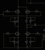
He is referring to your circuit drawing post number 21. There is a mistake
That circuit is designed for dual polarity power supply.
You need to make changes if you are using single ended power supply.
You need to make changes if you are using single ended power supply.
I would just use one trimpot on q1/q2 not 2, but you could add separate 3 ohm fixed resistors at the source of Q1/Q2 to balance current sharing.
Confused again. Did you mean to say use just one trimpot instead of two as source resistor at Q1 and Q2 and to use 3 Ohm source resistors at Q3 AND Q4( not Q1 AND Q2)?I would just use one trimpot on q1/q2 not 2, but you could add separate 3 ohm fixed resistors at the source of Q1/Q2 to balance current sharing.
I am planning to use dual polarity supply.
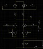
Referring to circuit in post 24.
Make R5/R6 10 Ohms each.
Make R7 R8 5 Ohms each then a single 5 Ohms trimpot in series.
As an example.
Make R5/R6 10 Ohms each.
Make R7 R8 5 Ohms each then a single 5 Ohms trimpot in series.
As an example.
If devices all have same idss then total effective resistance will be 5 ohms at the source.
Make R16 5 Ohms and P1 100 Ohms.
Set P1 to midpoint to start offset procedure.
If you need more adjustment increase R16 to 10 Ohms, but that should be adequate if reasonably matched.
Make R16 5 Ohms and P1 100 Ohms.
Set P1 to midpoint to start offset procedure.
If you need more adjustment increase R16 to 10 Ohms, but that should be adequate if reasonably matched.
Last edited:
Now if your BF862 devices have Idss values less than 15mA, I would suggest halving the resistance values.
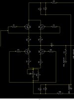
let's start with the circuit shown in post11.

Q3 is the constant current source.
Q4 is the source follower.
Let's assume the two devices are identical.
set R14 to 0r0.
The Q3 CCS runs at Idss and draws that current through Q4.
The Vds of Q4 is identical to Vds of Q3, i.e. no output offset. And C3 is not required.
Id of both devices are identical. Pq of both devices are identical.
That's how a B1 operates.
Now introduce a source resistor into Q3, that reduces the Id to some value less than Idss.
The current through Q3 equals that through Q4 and since it is less than Idss there will be a voltage across gate and source. This is Vgs. This is the output offset.
Now add a source resistor to Q4 as described by D.Feucht
This cancels the output offset and once again Pq of the two devices becomes equalised.
Staying with the D.Feucht version with upper and lower source resistors.
If the two devices are identical then the two Rs are also identical for zero output offset. and that maintains the equality of Tj because Pq are equal.
Now we progress to the question asked:
Do the devices need to be matched?
No, is the simple answer. But you lose the beauty of B1 and you don't have the zero offset of the D.Feucht
You can add a trimmer instead of a fixed resistor. That solves the output offset. But it introduces an inequality in the Vds. Adjusting the trimmer forces one or other of the devices to run with a high Pq and that ruins the equality of Tj.
The closer you match the devices the closer the two source resistors become and the close the Pq become and the closer the Tj become.
Now let's go single ended.
Insert the input and output DC blocking capacitors.
Two identical devices will operate at the same Tj.
Two non identical devices will operate at different temperatures.
Trimming to bring the output offset to a notional zero, (not actually required because there is a capacitor to block the DC) introduces the different Vds and thus unequal Tj.
Alternatively one could trim Rs to bring the Vds to be equal. Does this make the two devices behave identically?
Last edited:
My attempt to include the image from post11 has failed.
Can someone show me how to copy that left side sch into my post?
Can someone show me how to copy that left side sch into my post?
Andrew,
What is Pj and Tj and how they are important in design?
So it seems like the DC offset will be blocked by CAP C8. So a trimmer is not necessary even if the devices are not closely matched as long as a DC blocking cap is present?
I still have not got the answer from anyone about how Andrew Russel came with resistor value 49 ohm. Is he operating the Jfet in ohmic region Where Jfet act as resistor vs saturation region where it is a current source?
Last edited:
Pj = power at the device junction
Tj = temperature at the device junction
Two devices develop less distortion when they are identical.
A change in temperature changes the device parameters. Changed parameters equals non identical performance = distortion.
I believe that is what makes the B1 beautiful.
Tj = temperature at the device junction
Two devices develop less distortion when they are identical.
A change in temperature changes the device parameters. Changed parameters equals non identical performance = distortion.
I believe that is what makes the B1 beautiful.
- Status
- Not open for further replies.
- Home
- Amplifiers
- Pass Labs
- Another B1 design