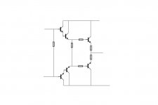
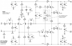
A little more than a darlington, it s a triple emitter follower.
Since there s no resistors on the emitter s of
the transistors that are in the middle of the arrangement,
the crossconduction range around the 0V crossing point
will be somewhat wider..
Also, the lack of this resistors make it imposible to discharge
the stored charges if even the transistor is driven to saturation,
wich is not a poblem in this case as they are fed from the same
supply voltage that their drivers, so they can t be driven to saturation.
I wonder why there are no cascoded driver stage to find anywhere?
Because there is usually no point in adding a cascode... A cascode helps much for common-emitter stages, but typically far less for common-collector configurations. Input Z of these is more determined by load and hFE rather than Co and Early effect.
Samuel
A cascode helps much for common-emitter stages, but typically far less for common-collector configurations.
Ah, ok
And a cascode driver stage cannot be common emitter ?
A little more than a darlington, it s a triple emitter follower....
The question in post #1 was about driver stage, and it's just a Darlington (although, a poor one)
A cascode generally has the emitter of one device connected to the collector of a second, whereas in your first circuit the emitter connects into the base of the second.
Of course you can build the circuit with FETs, where it's source->drain, or valves, where it's cathode->anode.
Just because you see the devices stacked in this way, it does not necessarily mean that the circuit is a cascode.
As with most circuits, it's worth googling them and looking at wikipedia... cascodes are characterised by a high input impedance and high frequency response, the latter due to the minimisation of the effect of Miller capacitance.
w
The question in post #1 was about driver stage, and it's just a Darlington (although, a poor one)
Agree, but the behaviour due to lack of emitter resistors
is still valid...
You might look at Nelson's article on cascode amp design especialy on page 4 of the
pdy. Go to passdiy.com . Look in the articles section.
pdy. Go to passdiy.com . Look in the articles section.

No, tinitus. This is FUBAR.
What are you trying to achieve?
Do you actually need a circuit for something, or are you just trying to get an idea of how things are designed, or what?
The best way to learn design is by learning how to arrange transistors in standard prototypes. Nobody invents a configuration, or at least very rarely; although genuine re-invention is inevitable there's not much that hasn't been tried. Most of the chains and cascades of transistors you see are simply stage after stage of standard configurations tied together in more or less conventional layouts.
You start with the common emitter and the emitter follower in the case of BJT's. You learn how to bias the common emitter, and how to analyze it in both DC and AC terms and what emitter bypassing and degeneration do to gain and stability. As you perform these calculations and try to understand how amplifier circuits work, and attempt to extend what you have learned to FETs and tubes, so you will also develop an understanding of how PNP devices mirror the function of NPNs in circuits with a negative supply rail.
w
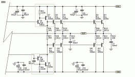
Thanks, maybe this is closer
I have no idea why a PNP drives NPN
But seems to be normal that way
There something wrong with that cct. The second transistor on the bottom is wrong (its always off). Its base voltage needs to be raised up at least 2 volts. What this does is keep the Vce and the load of the trans. before it constant.
Look at common base configurations. The cascode can be looked at as a 2 stage amp, common emitter feeding a common base.
Last edited:
What are you trying to achieve?
Trying to figure out how little I know, and that my DIY days are numbered 😀
I have 8 pairs of MJL21193/94
Maybe I wanted to use them in a Dx
Maybe with a cascoded driver stage, but seems impossible
But would be easier to just use a tougher driver
But as someone said, it will blow up in my face
I give up, and will look in a different direction
If anyone else want to use this thread, be my guest
But any suggestions are welcome, ofcourse
thank you all
Attachments
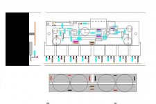

Ahh  I could just use the "standard" board to drive the 4 output pairs, at low +/-25Vdc, it would drive 1ohm ribbons without sweat
Im building ribbon tweeters right now, so it would be a convenient amp to have 🙄
I have all the output pairs, and a couple of heatsinks
And trafos would fit F5, if it doesnt work 😀
I could just use the "standard" board to drive the 4 output pairs, at low +/-25Vdc, it would drive 1ohm ribbons without sweatIm building ribbon tweeters right now, so it would be a convenient amp to have 🙄
I have all the output pairs, and a couple of heatsinks
And trafos would fit F5, if it doesnt work 😀
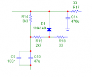
Still "working" on it, making small changes 🙂
Ah, maybe I will figure out this bootstrap diode, suggested by BV
Not sure why I connected bootstrap to ground, obviously a mistake, and should be connected to output
Corrected and hopefully better now
Probably more mistakes to find
Ah, maybe I will figure out this bootstrap diode, suggested by BV
Not sure why I connected bootstrap to ground, obviously a mistake, and should be connected to output
Corrected and hopefully better now
Probably more mistakes to find
Attachments
This look interesting tinny , 1 ohm ribbon tweeter , try for the whole ribbon ....😛
Nah, Im a chicken, and will try with 2ohm first 😀
Actually, like any other tweeter, my ribbon may need some attenuation, but Im not sure how a 1-2 ohm resistor will affect a zero ohm driver
But lets call it a "experimental project" 😛 but I guess the heatsink will tell if it can take the load


- Status
- Not open for further replies.
- Home
- Amplifiers
- Solid State
- Amp to drive 1ohm ribbon, using Dx