Hi Andy,
In circumstances such as this, JPS64 gives multiple options for a given location.
As an example, for the input cap you can use a fancy 10uF film cap, a Wima 10uF box cap or a Silmic ll 10uF cap. The 0.1uF could be a film bypass if an electrolytic cap is used.
Your free to pick what you want to use 🙂
Aah, thanks, Vunce. 🙂
Andy
I have never used a Class A amp on an active setup before but seeing AndyR’s possible use of it on an active system I thought I would give it a try. I am also testing out a new DSP from Dayton, the DSP-408. Very easy to setup with a simple 1 page app and no drivers to load. Using Alpha Nirvana for the woofer on a 5in PMC TL clone with an APA150 Class AB on the tweeter. Using a Harsch quasi transient perfect XO at 2kHz. The sound is impressive and the Alpha Nirvana drives the woofer with authority.
More on speaker here:
Low-Cost PMC-inspired TL Monitor with DC130A and DC28F
Video of testing speaker with Alpha Nirvana as active amp here:
XRK Audio on Instagram: “Testing out new Dayton DSP-408 on 5in foam core PMC clone TL’s with 40w Class A Alpha Nirvana amp and APA-150 amp for tweeters. Using…”

Hi X,
I have nearly finished modifying the BoM with the 4R version component values (which, of course, need Hugh's component numbering scheme! 🙂 ).
This has taken me several days - for 2 reasons 😡 :
1. I have had no internet access for most of the time since last Thursday, and
2. Comparing:
* Hugh's 4R cct diagram
* with his 8R cct diagram
* and your 'As Built' schematic - which has modified component values and JPS64's numbering scheme
... has been a nightmare! 😱
Before I can finish the s/sheet, I'm afraid I need some answers from you:
1. Vunce explained that JPS64's numbering scheme allows different options for some components - eg. choose 1x 10uF component from C102/C103/C104/C105.
Q1: are V113 & V115 simply 2 different options for that transistor?
Q2: if so, I'm curious how they can be interchangeable - given the BoM describes V113 (KSC3503) is rated at 0.1A ... whereas V115 (TTC004B) is rated at 1.5A?
2. Your 'As Built' schematic has R136 (4R7). This doesn't appear on either of Hugh's 4R or 8R cct diagrams. So:
Q3: I presume R136 actually does something useful (essential!)?
Q4: given it's required for the 8R circuit ... I presume it is also required for the 4R circuit?
3. Likewise, your 'As Built' schematic has C134 (2200pF). This doesn't appear on either of Hugh's 4R or 8R cct diagrams. So:
Q5: I presume C134 actually does something useful (essential!)?
Q6: given it's required for the 8R circuit ... I presume it is also required for the 4R circuit?
Thanks,
Andy
Hi AndyR,
When asking questions about a schematic, please post link to image inline with your post like this:
It will save me from having to dig through the thread to find it. Truth is, I do most of my responses to posts via my phone. I don’t have paper schematics in front of me nor my main laptop with the big screen. So if you want an answer quickly, including the schematic will be helpful.
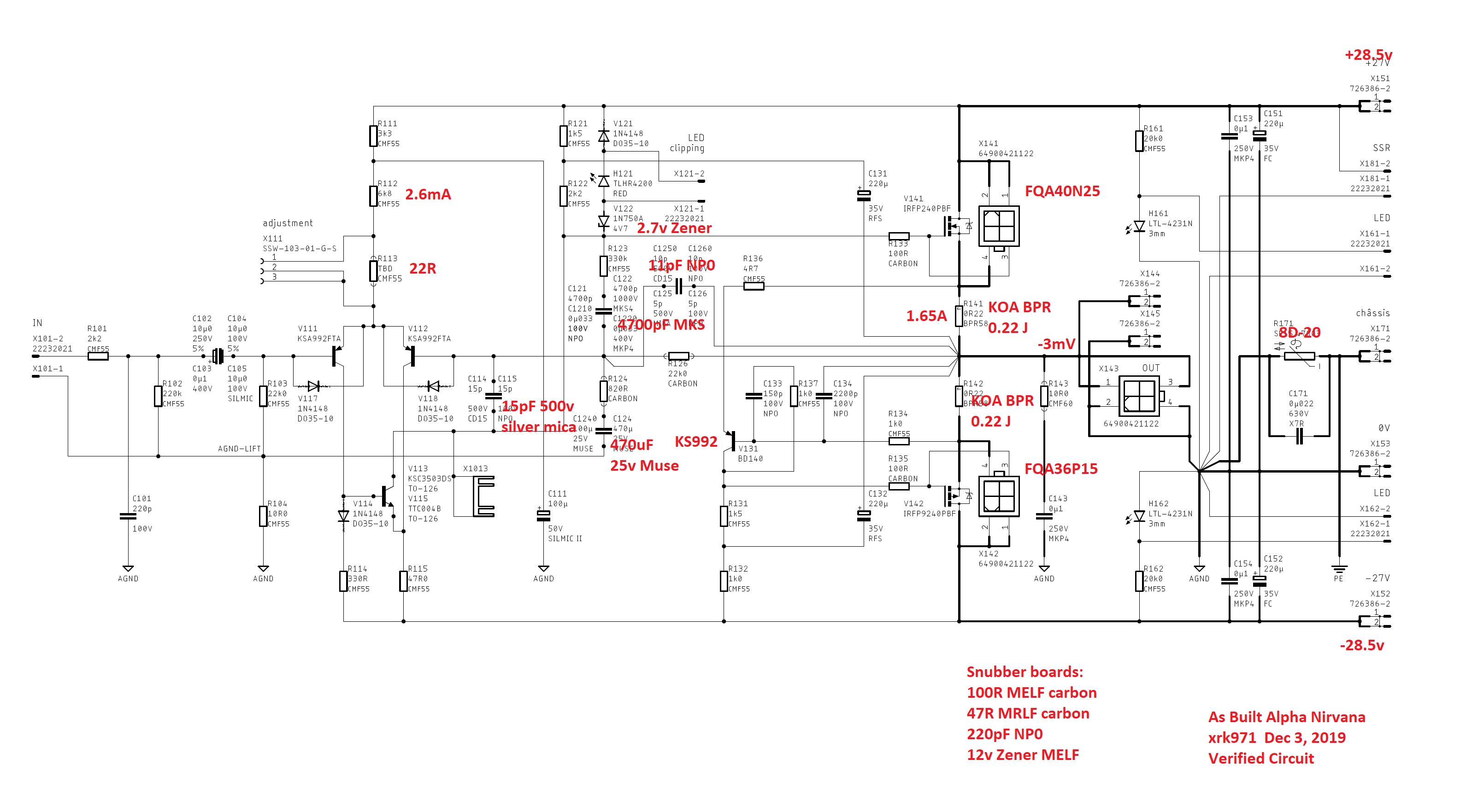
I am assuming that this is the 4R schematic you are referring to;
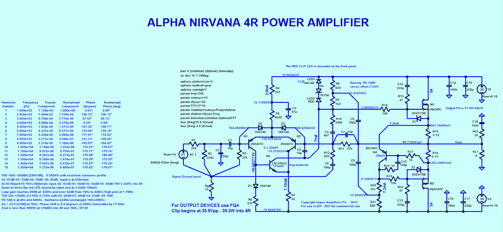
Let’s try to answer what I can, keeping in mind that some small changes to compensation tricks to prevent oscillation are added at the last minute via email requests and are not captured in Hugh’s final schematics which JPS64 uses for development of the prototype/production PCB. The questions you ask are partly related to this and partly related to fact that we try to provide alternatives for people regarding BJTs and MOSFETs.
You may ask this later: since the snubber boards have 100R gates stoppers already, is R133 and R135 needed?
Technically, no, you could use a wire jumper. But I installed 100R gate stopper on PCB and another on snubber board for a total of 200R gate stoppers. My thinking is that the stopper is on both ends of a flying lead that can pick up RF/EMi and maybe it will absorb oscillations better from both ends. That’s how it’s built anyhow and doesn’t oscillate. Change that and I can’t say it will not. Sonically, 100R lets the current drive higher capacitance of the MOSFET gate with more authority - perhaps higher slew rate. It’s DIY so you might try skipping g R133/135. I am not noticing any lack of resolution or slew rate though.
When asking questions about a schematic, please post link to image inline with your post like this:
It will save me from having to dig through the thread to find it. Truth is, I do most of my responses to posts via my phone. I don’t have paper schematics in front of me nor my main laptop with the big screen. So if you want an answer quickly, including the schematic will be helpful.
I am assuming that this is the 4R schematic you are referring to;
Let’s try to answer what I can, keeping in mind that some small changes to compensation tricks to prevent oscillation are added at the last minute via email requests and are not captured in Hugh’s final schematics which JPS64 uses for development of the prototype/production PCB. The questions you ask are partly related to this and partly related to fact that we try to provide alternatives for people regarding BJTs and MOSFETs.
Q1: are V113 & V115 simply 2 different options for that transistor?
Q2: if so, I'm curious how they can be interchangeable - given the BoM describes V113 (KSC3503) is rated at 0.1A ... whereas V115 (TTC004B) is rated at 1.5A?
Tested with KSC3503, but part is sometimes hard to find. TTC004 is rated higher but should work fine and well below its thermal limit. You could even use a KSC1845 here and it will work but is 175mW dissipation.
2. Your 'As Built' schematic has R136 (4R7). This doesn't appear on either of Hugh's 4R or 8R cct diagrams. So:
Q3: I presume R136 actually does something useful (essential!)?
It is extra precaution against oscillation - I would keep it.
Q4: given it's required for the 8R circuit ... I presume it is also required for the 4R circuit?
3. Likewise, your 'As Built' schematic has C134 (2200pF). This doesn't appear on either of Hugh's 4R or 8R cct diagrams. So:
Q5: I presume C134 actually does something useful (essential!)?
Again, extra belts and suspenders to guard against oscillation requested by Hugh at last minute of layout work to prevent Q4 from blowing up the outputs. 🙂 I would keep it. You are welcome to not use it but use an Oscope to check for oscillation. Of course, your MOSFETs may already be toasted.
Q6: given it's required for the 8R circuit ... I presume it is also required for the 4R circuit?
I’ll let Hugh answer but my guess is that it’s even more important in an a 4R application.
You may ask this later: since the snubber boards have 100R gates stoppers already, is R133 and R135 needed?
Technically, no, you could use a wire jumper. But I installed 100R gate stopper on PCB and another on snubber board for a total of 200R gate stoppers. My thinking is that the stopper is on both ends of a flying lead that can pick up RF/EMi and maybe it will absorb oscillations better from both ends. That’s how it’s built anyhow and doesn’t oscillate. Change that and I can’t say it will not. Sonically, 100R lets the current drive higher capacitance of the MOSFET gate with more authority - perhaps higher slew rate. It’s DIY so you might try skipping g R133/135. I am not noticing any lack of resolution or slew rate though.
Last edited:
Thanks Alan. Happy Xmas and a great new year to you too!
You mean VR46 is the GOAT? Yes.
Same with Messi in football.
You mean VR46 is the GOAT? Yes.
Same with Messi in football.
Thanks X, Andy,
Yes, you have to be very careful with the high current, loZ 4R variation.
Alan,
Thanks for your best wishes, the very same for you, and your family......
Stay well, and keep riding motorcycles (me too, I'm considering buying a Triumph).
Hugh
Yes, you have to be very careful with the high current, loZ 4R variation.
Alan,
Thanks for your best wishes, the very same for you, and your family......
Stay well, and keep riding motorcycles (me too, I'm considering buying a Triumph).
Hugh
Hi AndyR,
When asking questions about a schematic, please post link to image inline with your post like this:
It will save me from having to dig through the thread to find it. Truth is, I do most of my responses to posts via my phone. I don’t have paper schematics in front of me nor my main laptop with the big screen. So if you want an answer quickly, including the schematic will be helpful.
I am assuming that this is the 4R schematic you are referring to;
Let’s try to answer what I can, keeping in mind that some small changes to compensation tricks to prevent oscillation are added at the last minute via email requests and are not captured in Hugh’s final schematics which JPS64 uses for development of the prototype/production PCB. The questions you ask are partly related to this and partly related to fact that we try to provide alternatives for people regarding BJTs and MOSFETs.
Sorry for not including the schematics, X. 😱 You picked the right ones. 🙂
I will include R136 and C134.
You may ask this later: since the snubber boards have 100R gates stoppers already, is R133 and R135 needed?
Technically, no, you could use a wire jumper. But I installed 100R gate stopper on PCB and another on snubber board for a total of 200R gate stoppers. My thinking is that the stopper is on both ends of a flying lead that can pick up RF/EMi and maybe it will absorb oscillations better from both ends. That’s how it’s built anyhow and doesn’t oscillate. Change that and I can’t say it will not. Sonically, 100R lets the current drive higher capacitance of the MOSFET gate with more authority - perhaps higher slew rate. It’s DIY so you might try skipping g R133/135. I am not noticing any lack of resolution or slew rate though.
Thanks, X - I don't have enough technical knowledge to query whether R133/135 are still needed! 😀
I do note, though, that your snubber diagram - attached - shows:
* R101
* R102, and
* C102.
Can I suggest these component numbers are confusing - as the same numbers are used in the amplifier cct diagram and BoM.
Rather than leaving out R133/135 - what do you say to the suggestion of:
* including them on the PCB.
* then, during checkout of the working amp, short across these resistors whilst looking at the output on a scope.
* if no oscillation is noticed with R133/135 shorted ... try a listening session without & with R133/135 shorted, to see if resolution improves with them shorted.
* if not ... leave them in circuit (not shorted).
Andy
Attachments
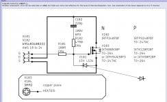
I agree the component designations are confusing since duplicated in the main amp. I guess this was a separate project from the Alpha Nirvana rather than part of the same set of schematics.
Your plan for testing with/without snubbers on board sounds good.
Your plan for testing with/without snubbers on board sounds good.
Thank you very much, Andy, this looks terrific, and with careful options for just about everything people could wish!
Hugh
Hugh
I just had an interesting thought. I could populate a new board as 4R and pop it into my existing amp with a different power trafo. Or maybe keep it and add some cooling fans to try out the 4R pretty easily. The quick connects on the MOSFETs lets one do something like that easily. If no power trafo change, the whole operation could be done in 5 minutes. Which leads to the next observation. Perhaps all future amps should follow this board format? Imagine trying out a brand new amp topology in 5 minutes of chassis work?
I just had an interesting thought. I could populate a new board as 4R and pop it into my existing amp with a different power trafo. Or maybe keep it and add some cooling fans to try out the 4R pretty easily. The quick connects on the MOSFETs lets one do something like that easily. If no power trafo change, the whole operation could be done in 5 minutes. Which leads to the next observation. Perhaps all future amps should follow this board format? Imagine trying out a brand new amp topology in 5 minutes of chassis work?
Surely a power traffo change is required, X - as you need +/-20v DC rails, for the 4R version.
That means 18v secondaries feeding the SLB PSs, right?
300VA on each channel - or, given the 3a current draw, 400VA?
And I would think you certainly would need 4x fans for the 4R version, with the same heatsinks. Or (better?) CPU coolers.
Andy
You certainly spent some time on the 4R version of the BOM Andy, well done.
Yes, I found it a struggle, gary! 🙂
A couple of times I felt like giving up and cancelling my PCB order ... but, luckily, was able to keep going.
A very happy Christmas to you.
Andy
Andy,
If you dimension the amp for 4R but run it from 25V rails you could use the same trafo but adjust the voltage drop across the SLB to amend the voltage. The SLB would drop a bit more watts, but if the amp was well cooled the higher rails would be OK and it could give you more than 60W into 4R.
X's idea is a very good one, and JPS's layout makes this all quite easy.
Hugh
Andy,
If you dimension the amp for 4R but run it from 25V rails you could use the same trafo but adjust the voltage drop across the SLB to amend the voltage. The SLB would drop a bit more watts, but if the amp was well cooled the higher rails would be OK and it could give you more than 60W into 4R.
X's idea is a very good one, and JPS's layout makes this all quite easy.
Hugh
Thanks, Hugh.
But I suspect in my set up - where one channel of each AN 4R will be driving a 3ohm mid panel with the other channel driving a 2ohm ribbon - it is advisable to stick to the +/-20v rails?
Andy
Andy, your BOM will be invaluable, I will use it as a reference for an 8R build.
Thanks again.
Seeing as I already have your email address, gary ... I'll send you the 8R s/sheet. 🙂 (More useful than the pdf version I attached to one of my posts.)
Andy
- Home
- Amplifiers
- Solid State
- Alpha Nirvana 39w 8ohm Class A Amp