I did this late last night and was exhausted.
2x20V rail gives as 40V to play with but we lose 5V to mosfets Vgs and a little to the current sense.
This leaves us 35Vpp max output so long as current holds out.
If the current is 1.67A quiescent then max current on negative half cycle is just under 3.33A.
Assuming a 6R load and ignoring reactive impedances this requires 6 x 3.33 = 20Vpk.
So current supply is fine (which should be ok for most speakers) and you should be about to reach 35Vpp into 6R.
That would be 25.5W and that should be correct now that my brain has recovered.....
HD

Hugh, thank you very much for your time!
With these data I understand that this 20w//8R version fits perfectly with this speaker project. I will also be able to use a 3U case with Heatsinks 120mm Height x 40mm thick x 400mm deep...and less heat, perfect! 🙂
Best regards
With these data I understand that this 20w//8R version fits perfectly with this speaker project. I will also be able to use a 3U case with Heatsinks 120mm Height x 40mm thick x 400mm deep...and less heat, perfect! 🙂
Best regards
What value are you guys using for R113 is it still 22R and no need for adjustment ?
Thanks
Scott
Thanks
Scott
@bigaudioscotto
This is what I did:
I measured the input stage bias by placing my voltmeter across R111 (3k3 CMF55 resistor), while carefully watching what my other voltmeter on the output of the amplifier was with regards to DC offset. Ideally, you want something with reasonably low DC offset (less than 20mV is fine), and bias to be around 2mA. Use V=IR to calculate what voltage you would need across R113 to get that bias. 22R is what X got with his prototype. It's going to be a little different for every build. You will want to use a pot for R113 if that is not clear. See the schematic. I think mine had a 200 ohm pot.
We'll see what the others say.
Best,
Anand.
Last edited:
Do the Ksa992 pair need to be matched in this Alpha Nirvana amp
Or are the ammo packs normally close enough in tolerance to be fine?
I installed these yesterday but It came to mind last night that it may be critical to match them
I will yank these back out and replace with measure ones if you guys think it's best?
Thanks
Scott
Or are the ammo packs normally close enough in tolerance to be fine?
I installed these yesterday but It came to mind last night that it may be critical to match them
I will yank these back out and replace with measure ones if you guys think it's best?
Thanks
Scott
You want the Hfe to be close and also to thermally couple them. It’ll ensure a low dc offset. In my original build, I had a long reel of 992’s and found a quad match quite easily. Post 2140 has some specifics of my build. If your dc offset is already low however I don’t think I would yank them out. Less than 50mV dc offset is fine in my book. The dc offsets in my personal build were between 1-3 mV.
See my pic here.
Best,
Anand.
See my pic here.
Best,
Anand.
Anand.
Yeah I have thermal coupled them,
I have not gotten to the finish line on it yet still have the snubber and
All the wiring to do so maybe I will just leave the 992 in there and see what I get when she is fired up.
Thank you
Scott
Yeah I have thermal coupled them,
I have not gotten to the finish line on it yet still have the snubber and
All the wiring to do so maybe I will just leave the 992 in there and see what I get when she is fired up.
Thank you
Scott
I don’t know if I would assume anything.
I would look at the schematic and trace it out:

Both C133 and C134 have one end connected to the base of the V131 transistor. Identify which pin of V131 is the “base.” Typically pin 3 for this type of transistor. You also know that C133 is connected BETWEEN the base of the V131 transistors and R137 (1k ohm). Once you have identified that, you are done.
Best,
Anand.
I would look at the schematic and trace it out:
Both C133 and C134 have one end connected to the base of the V131 transistor. Identify which pin of V131 is the “base.” Typically pin 3 for this type of transistor. You also know that C133 is connected BETWEEN the base of the V131 transistors and R137 (1k ohm). Once you have identified that, you are done.
Best,
Anand.
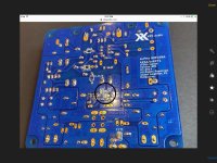
Well even after trying to trace this down about C133 and C134 I am still not
100 percent sure which is which but it seems that C133 is the one in the image that is on
The left side of the board with it corresponding number below it hopefully I am right on that
Help guys?
Thanks
Scott
100 percent sure which is which but it seems that C133 is the one in the image that is on
The left side of the board with it corresponding number below it hopefully I am right on that
Help guys?
Thanks
Scott
Attachments

Hello esteemed builders. I am a relative noob who has been slowly building my dual mono AN with SLB PSU in a Modushop 5U case. After doing a quick test of one SLB yesterday with no smoke or fireworks, I hooked up one amp channel this morning and was delighted to see LED's illuminate with no smoke or fireworks after 45 minutes. The FET's stabilized at ~69degC (measured on the snubbers), the SLB output was 28.7vdc which is a 2.8v drop across the transistors (I couldn't get it any lower). After dialing in the current across R111 to 2.73mA (by measuring 8.7v across it) I have 5mV offset across the outputs. All this seems good, but I'm measuring X111 at 672R, which seems out of whack. Can that possibly be right?
Yes, Scott, you are correct. But to be sure, remove one of the caps, measure it, then reinstall to be sure you have 150pF on one side and 2.nF on the other.
HD
JWC,
You are measuring X111 in situ, and your value will be some unpredictable. With 8.7V across 3k3 you have a nominal current of 2.64mA passing into the LTP input stage, which is close to 2.73mA, the designed value. A resistance at X111 will reflect the parallel 22R, which reduces its actual resistance to (672x22)/(672+22)= 21.2R.
The goal is to reduce the output offset to within about 10mV; no other requirement, so if it is met you are home free.......
You should not drop more than 2.8V across the SLB series regulator. It needs at least this voltage across it to accurately reduce ripple voltage and current pulses.
Congratulations, you are ready to audition!
Hugh Dean
Aha, I missed that extra bit of required math. Did I mention I'm a noob?
All this looks fantastic then, and the closest standard resistor value is 22R, so everything seems to jive. Excited to wire up the signal and output leads and get the casework finished.
For the SLB, for some reason I thought 3V was the goal, should I back that off to a smaller drop?
All this looks fantastic then, and the closest standard resistor value is 22R, so everything seems to jive. Excited to wire up the signal and output leads and get the casework finished.
For the SLB, for some reason I thought 3V was the goal, should I back that off to a smaller drop?
@JWCoffman
The actual output voltage of the SLB will vary from build to build. This has to do with a few factors. 1) The efficiency of your particular toroid transformer, 2) the output stage bias current of the AN, and 3) what your actual AC mains voltage is. When your AC mains voltage rises so will the DC output voltage of the SLB. Don’t worry it’s normal. The SLB is not a voltage regulator. It basically is a tricked out power supply for Class A amplifiers using a capacitance multiplier on the output to minimize AC ripple voltage to far lower levels than typical CRC supplies.
The drop in DC voltage across the BJT transistors you have currently sounds fine (and it‘s already set in stone by the BJT transistors themselves). The output pots are doing something different, read further…
Adjust the output pots on the SLB so that the positive and negative DC voltages are relatively equal and you’ll be fine (they vary the voltage very little, about 1V DC overall).
In actuality the output pots of the SLB should be adjusted for lowest AC ripple voltage which would require the use of an oscilloscope [and honestly, it’s academic since the voltage ripple is already very low for a Class A amplifier]. I am assuming you don’t have one, but that’s okay.
To make a long story short…You’re fine as is.
Best,
Anand.
Last edited:
Yes JWC, that would be my suggestion....
You will have a lot of support from this and other AN39 threads. There are some illustrious builders here!
The basic problem for the AN39 is thermal, not electrical. Each output device will continuously dissipate 47 watts of low grade heat, and you must control it to prevent the device surface temperature raising higher than 75C, heatsink no more than 55C. The purist solution is large passive heatsinks to prevent fan noise (around 350mmx150mm with 50mm fins for around 0.25C/W), but a practical option is using CPU heatpipes, close spaced fins and 120x120 slow speed fans - but with some noise. Each series regulating transistor will also produce around 6W per rail, so that has to be disposed with too.
There is the intriguing option of using the SJEP SemiSouth power jfet in the upper, nmos role. Pass describes much lower (10-20dB) distortion, and that is not to be ignored if you can source a couple of them. Poseidon/Anand knows quite a bit about this, but I would ask you please to make your conversations visible in this thread for others to follow.
BTW, you can also replace this nmos with a Sanken high dissipation NPN darlington, and that works too as AndyR on this thread has found.
Welcome to the AN39. Very good amplifier, and easy to build with excellent layout and carefully optimised for stunning performance. If you have speakers with 93dB/watt/metre sensitivity 40W would be more than you'd ever need.......
Cheers,
HD
Thank you so much for the response. I've gotten all the SLB output voltages equivalent (to within 0.1v at least), so I think I'm good there. Now it's just getting the rest of the work done to make it a functional amp.
Big thanks to you, AKSA, and XRK for everything. While I've yet to hear this amp, I don't think I'll be disappointed.
Big thanks to you, AKSA, and XRK for everything. While I've yet to hear this amp, I don't think I'll be disappointed.
- Home
- Amplifiers
- Solid State
- Alpha Nirvana 39w 8ohm Class A Amp