... Mouser Toshiba 2SJ74 data sheet shows BL suffix Idss of -6.0 to -12mA, so that makes the bdent Toshiba 2SJ74BL a grade B part, right?.
BL is what you're looking for. (More specifically as close to 8mA as you can get, IIRC.)
Thanks for your Reply...
What would be a maximum hi rail voltage for an Aleph J...
Someone will correct me if I’m wrong but I think it’s 30
After a search in the thread, I have gleaned that the JFET matching required is the Idss to be the same/very close for the JFETS within each pair.
Matching not required pair to pair.
I believe I can handle measuring Idss. Have 2 questions.
1. Anyone care to guess how many Toshiba 2SJ74BL's one should buy for a decent chance of coming up with 2 differential matched pairs (term from diyaudio store, do I understand it correctly?)?
2. Never found a tolerance figure to define "very close". Can anyone provide that for me?
1) 20-30
2) 5% is fine. Store matched is closer to 1%
1) Was afraid I'd hear something like that.
2) Sure wish the store had the differential matched pairs in stock.
Thanks for the info, 6L6.
This is my first DIY Audio project (not my first hifi project by any means) and I have been making a pair of monobloc 'J's, powered one up for the first time today. Getting +13v on the output which can be adjusted from +13 to +21 (+ve rail), R17 is running very hot and Q5 is running cooler than the other 3 power FETs. Any ideas where to look for the problem? Thanks, Phil
This is my first DIY Audio project (not my first hifi project by any means) and I have been making a pair of monobloc 'J's, powered one up for the first time today. Getting +13v on the output which can be adjusted from +13 to +21 (+ve rail), R17 is running very hot and Q5 is running cooler than the other 3 power FETs. Any ideas where to look for the problem? Thanks, Phil
This can be very frustrating but hold on. I had the same sort of problem and it turned out to be a cold solder joint (or two). I went over _al_ of the solder joints again - reflowing and adding where necessary. Also added a little more heat since I was initially trying to err on the side of caution.
During the troubleshooting I was asked the following:
First check the input stage. What is the voltage across R7? R8?
Output stage - bias across R18/R19?
Close up pics of the board also help - maybe someone can spot something like a wrong part.
Some have left out a jumper somewhere which then prevents biasing. So just go right through it carefully to make sure about that.
I took on board the advice to measure every resistor before fitting it. This would be a possible cause if you didn't. But if the value is clearly readable you should be able to check that carefully.
No doubt someone with more knowledge will be along soon.
They will definitely want some good clear photos.
It's going ! Resoldered a few joints to be ultra careful but bias was too high, 0.6v across resistors, so wound that down to 0.35 and then output offset could be brought to zero. Heatsink is running at about 45c, will put some more time on amp then bring bias up to 0.4v. Now for the second amp - phew!
Pass DIY Addict
Joined 2000
Paid Member
Congrats! This is an excellent reason to work on only a single channel at a time. If something goes wrong, you only risk one channel, not both.
I have seen somewhere here a diagram showing what to do to correctly integrate/change XLR and RCA inputs with a switch but can' find it now - can anybody help?
I have seen somewhere here a diagram showing what to do to correctly integrate/change XLR and RCA inputs with a switch but can' find it now - can anybody help?
No diagram at hand but it is easy to understand without one:
Connect GND of RCA and pin 1 of XLR to GND on amp
Connect + of RCA and pin 2 of XLR to + on amp
Connect pin 3 of XLR to - on amp
Connect terminals of switch to pins 1 and 3 of XLR.
Switch in BALANCED position: No connection
Switch in SINGLE ENDED position: Connect Pins 1 and 3 of XLR, shorting - to GND.
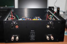
I do not have a photo of the inside, but this is how mine looks from the rear.
Attachments
Last edited:
Amp No.2 up and running. What does the variable resistor 'LTP Bias' do ? Haven't touched it but what does it do??
It sets the total current going through the diff pair Q1a/Q1b. Typically you
set it at 1K and forget it. You can just as easily use a resistor. (In fact,
I believe the original Aleph-J schematics has a 1K fixed resistor in that position.)
set it at 1K and forget it. You can just as easily use a resistor. (In fact,
I believe the original Aleph-J schematics has a 1K fixed resistor in that position.)
Thanks for reply; as amps seem to be working ok (not auditioned yet) I won't fiddle with it. Just a small amount of hum to chase down - wish me luck!
Thanks for reply; as amps seem to be working ok (not auditioned yet) I won't fiddle with it. Just a small amount of hum to chase down - wish me luck!
High efficiency speakers?
I get a tiny bit of transformer hum in the right channel, can probably solve it by turning the power transformer a few degrees but it's unobtrusive enough on my 86dB speakers that I haven't bothered.
- Home
- Amplifiers
- Pass Labs
- Aleph J illustrated build guide