Hi,
I am Mahesh from India. Last month i purchased aleph j pcb and mosfet kit from diyaudio store
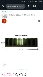
Attaching here with the spec of heatsink i just noticed in amazon.
Specs are as follows.
300mm × 100mm × 83mm (WLH). weighing about 2.7 kg / section and having thermal resistance of 0.12 C/W. Planing one section for each channel. I selected this because the one suggested by diy audio store for aleph j is 4u×300 mm chassis, its heatsinks are 300 mm × 165 mm × 40 mm (WLH). Which is having 2 kg per heatsink section and thermal resistance of 0.31C/W.
The one which i found in amazon is heavier than 4u×300 mm in diy audio store. Whether this section is sufficient for my project or i need to double the length from 100 to 200 mm on each section for each channel.
Expecting valuable feedback
Thank you in advance.
I am Mahesh from India. Last month i purchased aleph j pcb and mosfet kit from diyaudio store
Attaching here with the spec of heatsink i just noticed in amazon.
Specs are as follows.
300mm × 100mm × 83mm (WLH). weighing about 2.7 kg / section and having thermal resistance of 0.12 C/W. Planing one section for each channel. I selected this because the one suggested by diy audio store for aleph j is 4u×300 mm chassis, its heatsinks are 300 mm × 165 mm × 40 mm (WLH). Which is having 2 kg per heatsink section and thermal resistance of 0.31C/W.
The one which i found in amazon is heavier than 4u×300 mm in diy audio store. Whether this section is sufficient for my project or i need to double the length from 100 to 200 mm on each section for each channel.
Expecting valuable feedback
Thank you in advance.
Attachments

Give it a try, though I suspect that 0.12 C/W rating is rather optimistic. 🙂
If it gets too hot (for example with warmer weather), you can build a babysitter: https://www.diyaudio.com/community/threads/babysitter-for-papas-koan.186554/
Of course, you can also build a cooler 'summer amp'. (The AJ is one of the hotter FW amps.)
Have fun.
If it gets too hot (for example with warmer weather), you can build a babysitter: https://www.diyaudio.com/community/threads/babysitter-for-papas-koan.186554/
Of course, you can also build a cooler 'summer amp'. (The AJ is one of the hotter FW amps.)
Have fun.
I am hoping someone can help me. This is my second attempt at building an Aleph J. I couldn't get one of the first set of boards working so I re-ordered everything and tried again. I have one board working and one board drawing way too much current. I use a variac to test my circuits and on the bad board when I turn the variac up to about 7 volts ac, the circuit draws 1 amp from the wall (120 volt outlet). This gives me 1.26 volts DC positive and negative at the board. At this voltage I am measuring 520 mA across each of R16, 17, 18, an 19. I briefly turned the voltage up high enough to have 1.5 amps across each of the 0.47 ohm resistors. They quickly became very hot. I have triple checked all resistors, and transistors to make sure everything is in the right place. Triple checked for shorts and solder bridges. I have replace D1 and checked to make sure that none of the mosfets are conducting to the heat sink. I have stared at the schematic for hours but I don't understand enough to figure out what is going on. When I adjust the voltage on the good board to 1.26 volts, the current across R16, 17, 18, and 19 is Zero. The current drawn from the wall is also zero. Any thoughts would be appreciated.
Dan
Dan
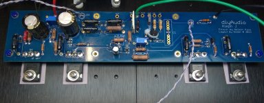
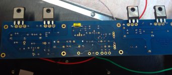
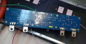
What's going on around D1? Is that the remnant from your replacement?
What's happening with R6? Did you jumper around it? That may be what I'm seeing.
Why no jumper in R30? What value is there? I assume that's consistent for all the boards.
Check to be sure that you have +- 24V (or close) from the PSU at full mains, and that the PSU is connected properly. If you have the rails reversed... it might look like that... ask me how I know...
If you want, ramp up the rails slowly on the working board and observe how the voltage across the source resistors goes up, then down and at what voltages it makes the 'turn'. Then...
With the board you're checking ... power it up slowly again with the Variac. As soon as you hit 100mV across the source resistor turn the bias down just to see which direction makes it go down vs. up. As you gradually increase the rail voltage, the bias voltage will increase a bit, then it should come down, and then it should stop at be roughly stable. Keep turning the pot keeping the value <300mV. Once you've reached your target rail voltages (assuming everything looks good) and know that there are no other issues with the board, you can ramp the bias back up to your desired setting. It might give you some peace of mind vs. just cranking it up. If the voltage gets too high with the pot fully cranked to the "lowest" bias ... then you've got other issues to investigate. Shut it off and pause.
Just a few ideas... it's how I'd do it, but... I also once smoked the current limiting device by hooking up the rails backwards... so...

Thanks ItsAllInMyHead. Yes, the mess around D1 was me replacing it.
That is a jumper around R6.
R30 is a 10 ohm resistor. Same on both boards.
It is getting late here now. I will try your ideas tomorrow morning.
Thanks again.
That is a jumper around R6.
R30 is a 10 ohm resistor. Same on both boards.
It is getting late here now. I will try your ideas tomorrow morning.
Thanks again.
Have you swapped the power supply connections to the boards, to see if the problem follows the board?
To defeat the Buzz, I'm going to try the 10 ohm resistor technique.The tweak with jumper in place:
10ohm and a cut trace
Can I cut the circuit across its entire thickness between GND and GND3? The circuit is on one side only at this location I believe?
For the resistance value, is 10 ohms required or are other values possible? I'll dig around to see what I have...
Even with this buzz, the sound is better as you told me. The sound was already not bad with the bad connection😅 but now it's magical.
Thanks for your help
Dan, I'm trying to understand what you did here. Is my understanding correct?
With the variac, you controlled the AC voltage so that on the bad board, you saw +1.26V DC on V+ ref GND, and -1.26V DC on V- ref GND.
You also measured approx 0.25V DC across the source resistors R16, R17, R18, R29 for about 520mA current.
If this is correct then with the same setup, can you measure the DC Vgs (gate to source) voltages of the big power mosfets Q5-Q8? These are the voltages across the two outer pins of the mosfets.
I have two 27.4 ohm resistors and I have two 0.47 ohms left... can they fit?To defeat the Buzz, I'm going to try the 10 ohm resistor technique.
Can I cut the circuit across its entire thickness between GND and GND3? The circuit is on one side only at this location I believe?
For the resistance value, is 10 ohms required or are other values possible? I'll dig around to see what I have...
Even with this buzz, the sound is better as you told me. The sound was already not bad with the bad connection😅 but now it's magical.
Thanks for your help
Thank-you everyone for your help. Turns out it was a bone head mistake. I swapped the board to right side power supply (the side that worked) as suggested by Mulburg, and the board powered up fine. (I am using a dual mono power supply) Turns out ItsAllInMyHead was correct and I had the polarity of the left channel power supply backwards. I won't be able to test the board until tomorrow to find out if it is working or not, but thanks again everyone, it's a big relief to finally find the problem.
^ Good news. It happens. If you hadn't been diligent... you'd have seen Q3? (don't have a schematic in front of me) go pooooooooooof as a self-sacrifice.
Nicely done ramping up slowly.
Nicely done ramping up slowly.
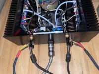
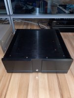
Thanks again for the help everyone. The left hand board powered up fine, and another Aleph J lives and breathes. Just hooked it up to my main system. Just a very slight hiss with my ear up against the 97db efficient speakers. Not at all audible from the listening position.
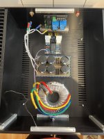
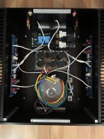
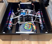
Another successful build from Aleph J thanks Mr. Nelson
Attachments


Hi guys,
I'm at a bit of a loss here. The amplifier runs and measures well.
However, I have a loud whistling noise that I can't get rid of. No matter if the inputs are open or shorted.
I suspect it has something to do with the ground, because if I place the heatsink just a few centimetres away from the chassis it is gone and the amplifier is completely silent.

Any ideas what else I could try?
I have replaced D1, transistors, jfets. J1/J2 fitted with 100ohm.
Changed the layout of the amplifier three times already.
I have attached a sound file. Attention it is loud.
I'm at a bit of a loss here. The amplifier runs and measures well.
However, I have a loud whistling noise that I can't get rid of. No matter if the inputs are open or shorted.
I suspect it has something to do with the ground, because if I place the heatsink just a few centimetres away from the chassis it is gone and the amplifier is completely silent.
Any ideas what else I could try?
I have replaced D1, transistors, jfets. J1/J2 fitted with 100ohm.
Changed the layout of the amplifier three times already.
I have attached a sound file. Attention it is loud.
- Home
- Amplifiers
- Pass Labs
- Aleph J illustrated build guide