Hi there. I’ve just received a new pair of JFETs from the Diyaudio store and they don’t appear to be as well matched as the two I just removed.. See attached pics of the new and old jfets. First two with long legs are the new pair. The old pair are within 0.01 and also appear to check out ok in the meter. Should I install the new JFETs ?
Mega328 has a bit of an issue reading Jfets in my experience. Both of your sets are absolutely good enough to be used without hesitation in your project. One pair just happens to be matched so well as to be incredible.
You’ll never hear the difference...
Replacement For Toshiba 2SK170/2SJ74 Post #412
According to Erno Borbely, +/- 0.5 mA Idss is a satisfactory match.
Ok, this got me thinking and I remembered another great trick I used during my days...
Whenever I suspected a faulty JFET with the symptoms as you have been having for a few weeks, this is what I used to do:
1. Insert few ohms’ resistors (same value for both, could be even 1 ohm): similar to degeneration resistors. This then allows me to measure the current through each JFET.
2. Touch with the probe, the gate of each JFET and then:
a) look for oscillations
and
b) look for an increased current run from common CCS, through a dodgy JFET that oscillates.
The above does not require removal of JFETS, with spot-on accurate results in finding a dodgy (slightly damaged) JFET
Same applies to figuring out the bad MOSFETS in the output stage; just touch the gate with a probe – the slightly damaged one will start oscillating like hell, and will pull much more current through its gate (source, depending on connection/circuit) resistor, compared to other ones.
Useful troubleshooting advice. I'll be filling this piece away in the "just in case" file.
Believe it or not, I was going to ask you to send the amp to me / Sydney to get it going for you... and then your email arrived saying it's all good... 🙂
re: heat, if the current draw through MOSFETS is correct, just place two of these underneath the amp:
Silent Series R3 120 mm — Fractal Design
Power them with 10V DC power pack (any). Dead quiet!!!... and will provide a lot of air circulation - a brilliant solution for class A (in Brissy) to leave ON 24/7.
Congratulations Roo2!
It might be interesting to see what a simple Idss type measurement will show on
your old jfets.
Enjoy your A-J.
Dennis
It might be interesting to see what a simple Idss type measurement will show on
your old jfets.
Enjoy your A-J.
Dennis
Believe it or not, I was going to ask you to send the amp to me / Sydney to get it going for you... and then your email arrived saying it's all good... 🙂
re: heat, if the current draw through MOSFETS is correct, just place two of these underneath the amp:
Silent Series R3 120 mm — Fractal Design
Thanks so much. Yes, I would have reached out tonight if the JFET replacement fell over. I’ll look into those fans. Definitely warming up here now.
Now that you are awake, can you please provide some much-needed enlightenment?
Can someone explain how would a different JFET saturation currents affect their usage in Alep J, please?
For example, one pair having Idss of 6mA (matched within 0.1mA tolerance margin)
....and...
the second pair having Idss of 11mA (matched within 0.1mA tolerance margin).
I read somewhere that the optimal Idss is around 8mA; is that true? Why is that?
Believe it or not, I was going to ask you to send the amp to me / Sydney to get it going for you... and then your email arrived saying it's all good... 🙂
re: heat, if the current draw through MOSFETS is correct, just place two of these underneath the amp:
Silent Series R3 120 mm — Fractal Design
Power them with 10V DC power pack (any). Dead quiet!!!... and will provide a lot of air circulation - a brilliant solution for class A (in Brissy) to leave ON 24/7.
I spotted this kit in my travels on the interweb recently:
AC Infinity Aircom Fans
I like its on board smarts for the capability of only needing to turn on when the temperature requires. If I needed extra cooling, I'd look into something like this, or at least consider it as an option.
Cheers
yeah , piece of drek preventing natural air flow , so it can switch on earlier
it is natural to place it (your own solution) beneath cooling assisted apparatus , not above
of course , when placed above , it's more dominant and easier to sell , another idiot gizmo
edit: so , if shown placed bellow , I wouldn't have anything to complain 🙂
it is natural to place it (your own solution) beneath cooling assisted apparatus , not above
of course , when placed above , it's more dominant and easier to sell , another idiot gizmo
edit: so , if shown placed bellow , I wouldn't have anything to complain 🙂
Last edited:
Yep. No carpet in my place. Old wooden floors with a few gaps in the boards for good measure.. Spring has sprung and it was ~32C today. Not hot yet😉
Now that you are awake, can you please provide some much-needed enlightenment?
Can someone explain how would a different JFET saturation currents affect their usage in Alep J, please?
For example, one pair having Idss of 6mA (matched within 0.1mA tolerance margin)
....and...
the second pair having Idss of 11mA (matched within 0.1mA tolerance margin).
I read somewhere that the optimal Idss is around 8mA; is that true? Why is that?
most imprtant thing is that Idss of JFet is greater than Iq , it have in LTP
due to CCS based biasing of LTP , Idss is having nothing with gain of LTP itself (value of loading resistor in JFet drain)
theoretically , Idss of JFet is having influence in THD spectra , same as value of it's drain resistance ( dependable of output mosfet's Vgs value) , but most of it is neutralized with NFB anyway , and it would require really Golden Ear (mein Bruder Generg?) to hear difference .......
in a word , there is most often just one rule applicable - Don't worry , be happy 🙂
What is “LTP”?
Thank you ZenMod!!
It appears that the CCS transistor steers the necessary current (around 8.3mA) through input JFETS to provide adequate voltage drop across drain resistor, to properly condition the output MOSFETS, so that they start conducting.
If we ignore the JFET's gate currents (and Kirchhoff’s Law), then each JFET runs at 4.3mA and 4mA.
So, why do we have to use the JFETS "in the range of 6-12mA"? That’s the bit I don’t understand.
What is the current / voltage drop (with no input signal), across the output "amplifieng" MOSFETS gate stoppers??
Last edited:
What is “LTP”?
Thank you ZenMod!!
It appears that the CCS transistor steers the necessary current (around 8.3mA) through input JFETS to provide adequate voltage drop across drain resistor, to properly condition the output MOSFETS, so that they start conducting.
If we ignore the JFET's gate currents (and Kirchhoff’s Law), then each JFET runs at 4.3mA and 4mA.
So, why do we have to use the JFETS "in the range of 6-12mA"? That’s the bit I don’t understand.
What is the current / voltage drop (with no input signal), across the output "amplifieng" MOSFETS gate stoppers??
back to basics , huh

google LTP , hope you'll end up on some prun site

please , ignore JFet gate current , but never ignore Herr Kirchoff
biasing each JFet at ~4mA , you ned to use those with Idss greater than said 4mA, from same reason why you're not trying to carry 2 sacks of cement , while you're able to carry just one ......... same as toobs (most of them) , JFets aren't on the best when driven with positive voltage at control pin ; then you have grid/gate current and then you have Berserked part ...... and we know that Berserker aren't too much predictable , in anything ; in fact , it's predictable that they are not exactly best behaving 🙂
(read - linearity suffers,badly)
mosfets are also having negligible gate currents , when idling ; even when modulated there is no actual gate currents but more "intrinsic capacitances pumping up/pumping down" currents , and these are more linear and predictable when you elevate enough Uds ...... gate resistor is there exactly to tame these currents at higher frequencies , to prevent poor part acting as confused switch
you'll not find all eenyweenytinybitsies in forum posts , better to find some comprehensive books
for starters , read all articles at FW , then find all amp books you can find from few resident (around) authors
and yes - on my blog you can download entire Papa Borbely's site
edit: you'll find very informative Papalectures at BAF ( OOtOObe) ; plenty of subjects explained swift and short , so even I could understand them ; sort of ; eeh ;🙄
Last edited:
back to basics , huh
google LTP , hope you'll end up on some prun site
These look potentially useful:
http://talkingelectronics.com/projects/TheTransistorAmplifier/TheTransistorAmplifier-P2.pdf
Chapter 12: Differential amplifiers [Analog Devices Wiki]
Last edited:
Yeah, of course. Just got a bit rusty on abbreviations.back to basics , huh
google LTP , hope you'll end up on some prun site
:
Of course not – that’s why I asked this question: “What is the current / voltage drop (with no input signal), across the output "amplifieng" MOSFETS gate stoppers??” But it’s all coming back to me now.please , ignore JFet gate current , but never ignore Herr Kirchoff
Thanks for your help…. I will build an Aleph J, measure the voltages I need to measure, and with help of the transistor specs sheets, the things will become clearer.biasing each JFet at ~4mA , you ned to use those with Idss greater than said 4mA, from same reason why you're not trying to carry 2 sacks of cement , while you're able to carry just one ......... same as toobs (most of them) , JFets aren't on the best when driven with positive voltage at control pin ; then you have grid/gate current and then you have Berserked part ...... and we know that Berserker aren't too much predictable , in anything ; in fact , it's predictable that they are not exactly best behaving 🙂
(read - linearity suffers,badly)
mosfets are also having negligible gate currents , when idling ; even when modulated there is no actual gate currents but more "intrinsic capacitances pumping up/pumping down" currents , and these are more linear and predictable when you elevate enough Uds ...... gate resistor is there exactly to tame these currents at higher frequencies , to prevent poor part acting as confused switch
you'll not find all eenyweenytinybitsies in forum posts , better to find some comprehensive books
for starters , read all articles at FW , then find all amp books you can find from few resident (around) authors
and yes - on my blog you can download entire Papa Borbely's site
edit: you'll find very informative Papalectures at BAF ( OOtOObe) ; plenty of subjects explained swift and short , so even I could understand them ; sort of ; eeh ;🙄
If you look at the transconductance curve of a JFET, it's flattest up near its Idss. I always assumed you wanted enough Idss to be over the top of what your CCS will deliver with a bit of error room, but not too much over so that you're operating in the less flat part of the curve.
However, I tried to model this in SPICE, and it didn't agree with my hunch, so I'm not sure.
However, I tried to model this in SPICE, and it didn't agree with my hunch, so I'm not sure.
If you look at the transconductance curve of a JFET, it's flattest up near its Idss. I always assumed you wanted enough Idss to be over the top of what your CCS will deliver with a bit of error room, but not too much over so that you're operating in the less flat part of the curve.
However, I tried to model this in SPICE, and it didn't agree with my hunch, so I'm not sure.
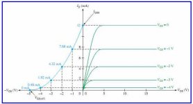
Is this the curve you are referring to (attached)?
Do you know what is the Aleph J JFETs' Vgs ??
Thanks,
Nick
Attachments
Last edited:
If you look at the transconductance curve of a JFET, it's flattest up near its Idss. I always assumed you wanted enough Idss to be over the top of what your CCS will deliver with a bit of error room, but not too much over so that you're operating in the less flat part of the curve.
However, I tried to model this in SPICE, and it didn't agree with my hunch, so I'm not sure.
you're right with that , say 90% of Idss is sweet spot , at least what Big Boys said .......
though , you always need to take broader picture in perspective - what's delta-I for part and how much of transfer characteristic you're using
not same situation with one vs. two JFets in parallel , same Iq
not same situation part processing line level signal , or phono signal
not same situation having NFB or not
- Home
- Amplifiers
- Pass Labs
- Aleph J illustrated build guide