Vref is like a Jung (or Jung/Didden) power supply voltage regulator, is all. Sometimes used for analog audio circuits with poor or non-existent PSRR.
could you check error amp inputs routing pls, i feel like i made mistake but brain is frozen whole day cant find it, probably elephant in room, i need a vacation.
Opamp wiring looks basically right. No offset pot is needed. Don't know if you have zener symbol for the diodes that could use it.
Regarding circuit operation:
Basically, there is a pass transistor that is biased on from filtered input voltage. An opamp can steal the transistor base bias and turn it more towards off. A zener is in series with the opamp output so that the output is offset lower and doesn't risk hitting its upper voltage limit.
The regulated output voltage passes through a voltage divider with speedup cap and is returned to the opamp inverting input for comparison with a zener reference at the non-inverting input. The zener reference and the opamp Vcc are powered from the regulated DC output.
Does that help explain operation? If not, please ask any questions you want.
Last edited:
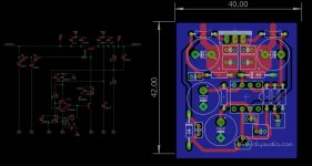
Forgot to specify, one of the goals of this project is to use SMD parts in as many locations as possible, to keep the boards compact, assembly costs low, and minimize parasitic lead inductance from component leads.

sry cant edit last post, here is isolator part of pcb, well half of isolator but other half same.
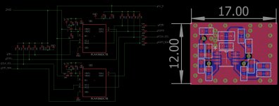
edited picture, sry for messy schematics.
also few questions.. please confirm, are diodes on VREF part supposed to be Zener or Schottky?
also is there reason that bypass caps on ISOLATOR part is before 200K resistor on VCC_R.
edited picture, sry for messy schematics.
also few questions.. please confirm, are diodes on VREF part supposed to be Zener or Schottky?
also is there reason that bypass caps on ISOLATOR part is before 200K resistor on VCC_R.
Attachments
Last edited:
...here is isolator part of pcb...
Pic is illegible.
The forum software will reduce picture resolution if file is 1MB or larger. If smaller than 1MB forum may or may not reduce resolution, but more likely that the pic will be left intact.
please confirm, are diodes on VREF part supposed to be Zener or Schottky?
The diodes are actually placed on the analogue supply pins, Vdd/Vss, not Vred, but the question about the Zener or Schottky confuses me too. The datasheet mentions placing Zeners at this location to breakdown if the supply voltage exceeds the breakdown and protecting the device.
Placing a Schottky here isn't going to accomplish the same task. The device will conduct if the negative supply voltage goes higher than the Vdd supply voltage, so essentially protects against reverse polarity on the Vdd pins.
They are Schottky. Part number is legible if the .pdf is opened Chrome browser (which has the needed fonts).
There are no protection zeners included on the eval board.
There are no protection zeners included on the eval board.
Yeah, noticed that a lot of parts don’t have PN’s when opening the pdf in reader, will go and backfill as much as I can today. Going to be out of the country visiting family for a couple weeks, will either have more/less time to work on this depending on the day, and then i’m leaving for college soon, but am aiming to have finished the eval board schematics and layout, and have an ALPHA release of the kicad project by the new year, not sure what to license it under though. I’d like a license that prevents commercial use, maybe with provisions to be able
to do group buys, although i would like to be able to keep it to a vetted list of organizers who can confirm electrical pcb testing, things of that nature, although fab houses can do that for a cost these days. However, for diy use, I want this project to be entirely open, anybody is free to modify, share, remix, just not sell the source files. Also likely a sharealike license. A software license probably isn’t appropriate for this project, any suggestions?
to do group buys, although i would like to be able to keep it to a vetted list of organizers who can confirm electrical pcb testing, things of that nature, although fab houses can do that for a cost these days. However, for diy use, I want this project to be entirely open, anybody is free to modify, share, remix, just not sell the source files. Also likely a sharealike license. A software license probably isn’t appropriate for this project, any suggestions?
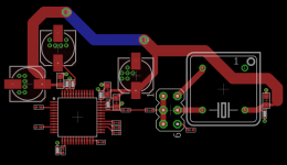
SRC part started, what type of connectors should i use for add in boards?
Wrong footprint and location for a clock.
The reference clock source should probably come from one of the dac chip clocks, depending on where they are located. Care should be taken to preserve clock signal integrity across any connectors and layout routing.
In other words, there will have to be some overall project coordination if multiple people are working on board layouts.
Last edited:
Markw4, agreed, there is a need for overall project coordination. I'm still very much in the schematic stage myself, but here's what I'm thinking in terms of some overall standards:
Thinking of using U.FL connectors for Clock / high speed signal distribution, and then am considering using PCI modules slotted into a backplane for different pieces of the DAC. I envision having a power supply card, maybe a clock card, and then likely a shared I/V + DAC card, thinking of using samtec board-to-board connectors to connect the two. Voltage regulation should be as close to the load as possible, meaning a lot of the regulation is going to have to be done outside of the power supply board. I know that trace length can become an issue with signals at this speed, but I figure that if they do it in high-end test equipment, they're likely onto something.
In terms of other standards, I would like community input on those. What works best for you?
u.fl connectors are my least preferred dac RF connectors. The shields are crimped with only a couple of thin flaps. The same single piece metal body also provides spring tension for the ground connection. If they are carefully inserted only once and never rotated in their sockets at all then they may be tolerable. The tool to properly plug them together is costs over $100, and the disconnect tool about $15 to $20. If they are not babied then after two or three times being plugged in and disconnected, time to replace them. Look at one that has been installed removed a few times, especially without proper tools. Put it upside down under a magnifying glass or microscope. What a piece of junk.
Also, LVCMOS cannot drive the capacitance of a 50-ohm transmission line. The rise time gets rounded very quickly unless they are first buffered by something like NB3L553. Terminators will be needed at one or both ends for transmission lines.
Much better if coax is really needed then go to SMA connectors for jitter critical clock signals. Otherwise, for short jumps of an inch or two, just use ribbon cable and gold plated pin connectors. Every other wire should be a ground. That works quite well for fairly high speeds and less capacitance for LVCMOS to drive. Series loading with a few tens of ohms works pretty well to control reflection effects.
Clock and I2S signals should be routed through an internal layer in a 4 or more layer board. See "Electromagnetic Compatibility Design" by Ott for excellent and practical advice, a goldmine of relevant info.
Last edited:
Also, LVCMOS cannot drive the capacitance of a 50-ohm transmission line. The rise time gets rounded very quickly unless they are first buffered by something like NB3L553. Terminators will be needed at one or both ends for transmission lines.
Mark,
Forgive me for another little 'nudge'..
There is no such thing as a 'transmission line capacitance'..
It's either terminated, and it is equivalent of a 50ohm resistor, (only real part of impedance), and no rounding of the edges.
If one terminate at both end, as it should be - then all the driver see is a 100ohm resistive load.
If there is no termination at either side, or improper termination (typical audio territory..) - then you have all type of reactances entering into the game..
But the real help for clean rise times is terminating, not brute force drivers..
Ciao, george
Hi George,
I will not quote you post, as it is too riddled with misunderstandings to possibly correct line by line. Also, I am not saying you are to blame, don't know where you picked all that up.
Regarding loading or terminating transmission lines, parallel termination of a uniform line in the characteristic impedance of the line results in no reflections from a terminated end (could be either or both ends). A source driving a source parallel-terminated line sees 1/2 the transmission line resistance, for a 50-ohm line it would be 25-ohms (not 100-ohms).
The reason an transmission like can appear to look capacitive or inductive, say, is pretty well explained in TDR references and hopefully understandable. For sine waves, explanation can be found in study of stub-tuned lines and use of the Smith Chart.
Whether or not a source can drive a line sufficiently well to produce a usable signal at the other end depends on the source's equivalent source impedance (and signal level of course). LVCMOS has a high-ish output impedance and cannot properly drive low impedance loads, transmission lines or otherwise.
Series termination is sometimes seen. It is sometimes used to help provide damping of reflections when a line is not or cannot be more properly parallel terminated. Sometimes we see series termination of short length lines that can be driven by LVCMOS. They are more likely nonuniform lines of short enough length and low enough capacitance (capacitance-per-unit-length times line length = total line capacitance) for a LVCMOS signal to work reasonably or passably well. Often such lines are found on PCBs or in very short length interconnects between PCBs. A not very much longer length of 50-ohm coaxial cable would be a very different situation for LVCMOS. In such case, conversion to another transmission format would likely required, perhaps such as LVDS (for one example).
In the case of DAC clock and I2S signals on PCBs and across interconnects, it has been found helpful in many cases to reclock (relatch) such signals due to rise-time rounding and other aberrations resulting from less than optimum transmission of the high impedance signals. That is the type of problem I would like to see us avoid across interconnects between the modules Adam would like to design for. More discussion of possible use of reclocking options should likely come up later when more thinking about where master clocks should be located comes more to the fore.
For uniform transmission lines, something like a short introduction to TDR might help explain part of the story about transmission lines and termination: http://www.tek.com/dl/55W_14601_2.pdf
Non-uniform transmission lines are a more general case, but hard to find tutorial reference information quickly. One possible source to study could be: http://www.jpier.org/PIER/pier71/06.07020801.Khalaj.pdf
Bottom line in this case, I stand by what I said. Happy to respond to any serious questions about it if people would like more clarification.
Regards,
Mark
Last edited:
Mark.. I'm only doing it daily.
And thank You, I know the literature. I have my personal TDR. But I use also our network analyzer (out of several) for real, not theoretical control of the situation.
I do not know, how it came into the picture, that 25ohm result for You.
The driver sees first the inserted series resistor (which has its task to terminate the line accross the driver output impedance) -which is usually 50 ohm. It can also be adjusted for the driver output impedance.
Then the correctly terminated tr.line presents itself like a real, resistive impedance to ground. 50ohm.
From ( an ideal, zero impedance driver) we see the two resistances in series, towards ground. 100ohm. That is the load for the driver.
Obviously, the signal amplitude is halved at the receiver side.
All the best, George
I do not know, how it came into the picture, that 25ohm result for You.
I think Mark was taking the 50ohm at the source end as a shunt R, whereas you are taking a 50ohm series. Mark's version only works without reflections if the driver has Z>>Zo (for example a current source). Your version halves the driver's output voltage which might not be terribly useful when logic levels are expected at the other end.
FWIW I think you might both be talking at crossed purposes here to some extent as Mark's 'disagreement' didn't seem that different from what you said originally George and which I happen to agree with. Which is that a transmission line with correct termination doesn't present a capacitance to the source, only a pure resistance.
- Home
- Source & Line
- Digital Line Level
- AK4499 DAC Design