Yes it appears that despite your use of a groundplane, a sufficiently big oscillation on the pass transistor's gate can produce quite a bit of delta-V between GND_at_lower_left and GND_ar_right_near_opamp. Picture 3 of post 398 confirms.
So it seems that you will have to connect scope ground clips to the little post northeast of the text "C11", to see what's actually happening on VREF. Previous waveforms were corrupted by hash on the croc clip "ground" over at lower left.
It's beginning to appear that VREF will probably turn out to be clean, and not the source of troubles. {which makes sense, because it's the same VREF whether the load is zero or 1.5 amps}. It's beginning to look like the feedback loop containing the opamp, pass device, and other contrivances... is probably going to turn out to be the sole culprit. This will be messy to probe because you'll want to connect your scope ground clip to one place when probing the MOSFET source, and to another place when probing all other nodes around the loop.
However the good news is, putting your finger on various components did have some effect, if I remember correctly. This gives hope that mortals might discover slight tweaks to the frequency compensation networks, which tame the oscillation, even with the volatile rocket fuel AD797 installed.
I think it's likely you will want to have a number of different values of capacitor CY on hand, for experimentation. Same goes for CZ, RY, and RZ. What values of those components bring the LTSPICE simulated unity gain crossover frequency down by a decade? Purchase parts of those values, and a couple smaller values, and a couple of bigger values. Spend the extra four dollars to have plenty of options. And if you're ordering by mail, this may be the time to get some just-in-case extra opamps or lower bandwidth opamps too.
If you are able to annihilate the oscillation completely, then you can try other values of load resistance (5A), you can try the chop chop box again, and so forth. You can verify that the thing works and is stable for "all load conditions" (that you tested).
Then if you are a greedy madman you can try to reclaim some of the bandwidth you discarded in order to make the circuit stable. Maybe you will be able to tiptoe right up to the cliff of death without falling over.
I agree with the conclusions of post # 400. It smells like VREF is ok and what is needed now is to probe each node with respect to its local ground. For the VREF network, that's the opamp GND pin or the little post 2cm away.
I don't think you'll learn anything useful by probing the rectifiers but if you want to, I'd put the ground clip on the D2-D3 GND and then go looking around. Set the probes on 10X and start at 20V per division to protect the amplifiers. Then ratchet the gain up to make the scope trace taller.
I don't think you'll learn anything useful by probing the rectifiers but if you want to, I'd put the ground clip on the D2-D3 GND and then go looking around. Set the probes on 10X and start at 20V per division to protect the amplifiers. Then ratchet the gain up to make the scope trace taller.
Well at the end of my 'heat mapping' I slipped and momentarily connected the op amp output and its supply join with my probe (they're right next to each other). (Memo to self, don't have a coffee before doing this stuff.) I fried the AD797. No more oscillations anywhere...
I will drop another AD797 (why not eh) in but dump the Zobel between drain and gate and use a 100R gatestopper.
On the other op amps, any thoughts as to which an increasingly conservative fellow might try first? How to evaluate? Need decent GBW and good slew rate, then low noise?
I will drop another AD797 (why not eh) in but dump the Zobel between drain and gate and use a 100R gatestopper.
On the other op amps, any thoughts as to which an increasingly conservative fellow might try first? How to evaluate? Need decent GBW and good slew rate, then low noise?
Attachments
Thanks for the reminder re #133; the commentary you provided there is very helpful.
I knew I might have to battle transient induced effects and was prepared to futz with Zobel vs gatestopper and the compensation network Cy and Ry, but this periodic bursting of distortion/oscillation under constant load seems to be something rather different. If it is still there when switching from Zobel to gatestopper I'm bailing from the AD797.
I knew I might have to battle transient induced effects and was prepared to futz with Zobel vs gatestopper and the compensation network Cy and Ry, but this periodic bursting of distortion/oscillation under constant load seems to be something rather different. If it is still there when switching from Zobel to gatestopper I'm bailing from the AD797.
I might be narrowing in the problem - or perhaps it's just obscured the old one (the periodic oscillation) temporarily. I replaced the op amp (and reconfigured the circuit from Zobel to gatestopper, adjusting the compensation resistor Ry to match my modelling). But I had 20V out as it was in last night. Perhaps I did't fry the op amp after all.
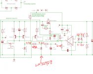
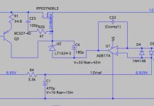
It seems the LM329 may have been the problem. See attached for measured voltages at various points in the circuit. With the LM329 in trouble, I don't see the oscillation previously witnessed on the output. Maybe the LM329 is the cause?
Before I replace the LM329 I want to double-check the pin configuration and its resistor value. R10 is 499 Ohms and my LTspice model suggests that this will mean 6.5mA through the LM329 which seems to be straight down the middle of its operating current. When looking at the board, I have the middle pin connecting R10 and R11 and the top pin going to ground.
Attachments
Wow! Input protection diode D6 is turned on hard (!!!) which pulls Vref up and squirts (10.4 - 3.2)/3300 = 2.2 milliamps into Z2. Ugh.
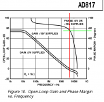
AD817A and AD825A ordered... I just hope they will work with the Zobel as a 100R gatestopper collapses modelled phase margin enormously.
Last edited:
I think it's likely you will want to have a number of different values of capacitor CY on hand, for experimentation. Same goes for CZ, RY, and RZ. What values of those components bring the LTSPICE simulated unity gain crossover frequency down by a decade? Purchase parts of those values, and a couple smaller values, and a couple of bigger values. Spend the extra four dollars to have plenty of options.
Yes, I am taking your good advice here. I think I have already parts enough to accommodate a decent amount of room for manoeuvre. I remodelled with the AD817A earlier today. With 100R/47pF Zobel it models plenty of phase margin with no need for Cy/Ry compensation. It may just sneak in with 100R in the gatestopper scenario without Cy/Ry compensation also - I have plenty of resistors try lower gatestopper values if needed and quite a few options if Cy/Ry is needed as well. I am looking at the AD825A again now. I recall this being much less accommodating when I looked at it some time ago. (I have paused my purchase basket until I complete this work.)
PS: out of interest, what temp do you use when doing this sort of soldering?
PS: out of interest, what temp do you use when doing this sort of soldering?
For 8-SOIC work, I use Kester #44 solder (63% tin, 37% lead) @ 0.5 mm diameter, a Hakko FX888 iron set to 375 degrees C, with a Hakko T18-D12 tip (1.2mm wide chisel).
I tin the corner pad on the PCB with the thinnest layer of solder possible, then position the IC with tweezers, then apply the iron to that pin+pad. Once it's connected I start at the diagonally opposite pin and begin soldering them down one by one, using the correct modicum of solder. I re-solder that first pin, which needs a wee bit more solder IMHO.
I tin the corner pad on the PCB with the thinnest layer of solder possible, then position the IC with tweezers, then apply the iron to that pin+pad. Once it's connected I start at the diagonally opposite pin and begin soldering them down one by one, using the correct modicum of solder. I re-solder that first pin, which needs a wee bit more solder IMHO.
Thanks. I have been using a lower temp, 280C, and was worried it was too high. My solder is 62, 36, 2 Sn, Pb, Ag in 0.56mm. (Same technique.)
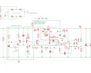
I'm going in circles with this. I swapped out the op amp to AD817A but still have the problem noted in #406 and so can't progress from there. Circuit with quick RMS voltage readings attached hereto.
Note the difference between the voltage at the +ve input terminal of the op amp (10.2V) and at the LM329 Z2 (7V). Also the difference in voltage at the gate of the MOSFET (21V) versus at the output of the op amp (12.5V); this difference should be 5V not circa 8.5V.
I presume Z3 is problematic but I replaced it earlier and hence I'm running out of confidence that this is indeed the issue. Before I try replacing it again, should I be checking other items? (Other than replacing virtually everything in one go...)
Attachments
It sounds like your PJFET doesn't match (this datasheet)
Using the red numbers in post #413 we can calculate the current in R8. Then if we temporarily assume that Q1, Q2, R7, and R8 are 100% functional parts in good working order, we can calculate the current in the PJFET. It does not match the IDSS for MMBF5460. Maybe your vendor shipped the wrong devices? Maybe the PNP current mirror subcircuit contains some broken parts?
I'd remove the 1.5 amp load, get rid of the oscillation, and go probing the DC values. Compare against a simulation at the same conditions. Compare against your idea of how things OUGHT to work. Maybe when you slipped and shorted some pins, that damaged the board or some components on the board. Go looking. Trust nothing.
Thanks
Q3 had failed, although in getting to this conclusion I also replaced J1 and Z3. I'm now back in business, so-to-speak. With the AD817A installed the oscillation witnessed previously is no longer there (1.5A load). I can now resume my load and transient testing. At least I am smiling again.
Q3 had failed, although in getting to this conclusion I also replaced J1 and Z3. I'm now back in business, so-to-speak. With the AD817A installed the oscillation witnessed previously is no longer there (1.5A load). I can now resume my load and transient testing. At least I am smiling again.
At least I am smiling again.
Well that was short-lived. I must be jinxed. I tested the board up to 4.5A. All seemed okay and so I connected my chop chop box. The MCP1407 went up in flames (literally). And something(s) went on the power board as well. So I am back trying to get the board up and running and will of course have to repair the chop chop box.

What values of those components bring the LTSPICE simulated unity gain crossover frequency down by a decade?
Question regarding this: What if lowering the unity gain crossover frequency doesn't increase phase margin?
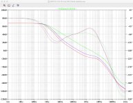
Attached is a Spice run varying the compensation capacitor from none (green trace), to 47p (blue) and then 100p (red). Unity gain crossover frequency falls but there's little if any phase margin gain (although gain margin improves).
Attachments
Last edited:
Maybe that telling you that the excess phase is occurring somewhere else in your circuit.
But since I can't use a sim package, my comment is probably worth ignoring.
But since I can't use a sim package, my comment is probably worth ignoring.
You are discovering that electrical engineering encompasses more than running SPICE.
I think it might be a good exercise to ask yourself "What would I do if I had to solve this problem all by myself?" Formulate a plan of action, execute that plan, and see whether you make forward progress.
I think it might be a good exercise to ask yourself "What would I do if I had to solve this problem all by myself?" Formulate a plan of action, execute that plan, and see whether you make forward progress.
Indeed, and clearly I have been struggling - less with the recognition that EE encompasses more than running LTspice but more as to how to grapple with what could be a multitude of compounding issues with the circuit implementation and my inexperience. So today I started methodically checking everything again starting with the basics of checking all the resistors with my multimeter again.
I believe the destruction of my MCP1407 was caused by supplying too high a supply voltage from the PSU rail - when the latter 'fails' it delivers 24V+.
With the PSU circuit board, I believed the problem had something to do with the current source/mirror - at the moment I have next to no voltage drop across R7-9 (as opposed to before when there was excessive voltage drop) - and the pathway from Z3-Q3 and Z3 to the gate of the pass transistor. My LM329 is delivering 6.95V but Z1 was down around 9V instead of 10. However, replacing the FET J1, PNP transistors Q1-Q3 and Z3 wasn't helping. I went back to the board itself. No obvious damage - pads and traces ok. I went back to my board layout file...
There's a schoolboy error with respect to Z3. I plonked down a Zener diode in SOT23 package just as I had for Z1. For Z1 it is fine/correct. But while the LM4040AIM3-5.0 components I have been fitting are a SOT23 package, the pin layout is different. I had basically connected the cathode to the op amp output and left the anode floating. Luckily it would seem that I can fix the issue by rotating the part on the board.
I'm still thinking about whether this is the full extent of the problem. Quite frankly, I'm baffled that I got 12V output at any moment previously. Currently, without Z3 repaired I have circa 14V RMS output from the op amp but 23V RMS at the pass transistor gate to collector of Q3 trace which suggests to me that more has gone wrong (perhaps because of the error with Z3) and rather likely Q3. (Annoyingly I have already blown through a very large proportion of my PNP transistors as I purchased only 10.)
Where I am particularly unsure of myself is whether I can repair things incrementally by which I mean correct Z3, test and proceed from there. Or is it likely that if other parts have failed (e.g. Q3) then leaving them failed will damage, for example, the new Z3 and hence I go round and round in circles. At the moment I think I can go incrementally.
With regard to my question in #417, I presumed the idea behind the suggestion was to 'detune' the circuit so that there was a very large phase margin, get it going and decide whether to push the boat out from there. But when I looked at the model it seemed like there wasn't a cushion to be gained. Of course if the model is wrong/incomplete then it's all a crap shoot anyway and most likely detuning things at least won't make matters worse.
Last edited:
- Status
- Not open for further replies.
- Home
- Amplifiers
- Power Supplies
- Adventures with 5A regulated voltage circuits