Read your voltages at Q1 pin 1,2,3 and Q2 pin 1,2,3
Compare left to right
The light coming on means the LED works, nothing more. We already know the PSU works because the other channel is good. 🙂
Q1 pin 1 is zero.
All others are jumping around....about 2 or 3 volts.
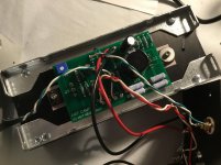
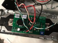
Could You show on the photo(s) what the PCB's looks now ?
Do You reflowed all mosfets as well ?
I reflowed everything.
I just mounted the PCBs back to heatsinks to test Q1 and Q2. Let me get iPad charged a bit and I'll take some more pics.
5 times that a lot !
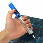
Normaly proper work You need clean old soldering point first.
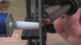
Use desoldering pump tool are the classic technique.
About soldering excellent video 🙂
YouTube
I need one of those. I would have thought that I could have gotten it right at least one of those attempts - at least to have corrected the issue. Maybe not with any style points, but still...
I've reflowed the board about 5 times now.
5 times that a lot !
Normaly proper work You need clean old soldering point first.
Use desoldering pump tool are the classic technique.
About soldering excellent video 🙂
EEVblog #183 - Soldering Tutorial
And desoldering
I need one of those. I would have thought that I could have gotten it right at least one of those attempts - at least to have corrected the issue. Maybe not with any style points, but still...
This video save You a lot of time and bring more successful DIY projects :
How to Desolder Through-Hole Parts, Why Some Joints are Difficult
Kind regards 🙂
Attachments
 in the near future
Yeah, I need easier. It went together fairly well, but now I’ve spent twice the time attempting to troubleshoot.
I appreciate everyone’s help, now if I can just find the problem.
It seems to me Q1 pin 1 shouldn’t read zero if every other pin on Q1 and Q2 have some sort of voltage.
But then again, I’m a newbie. 🙂
I appreciate everyone’s help, now if I can just find the problem.
It seems to me Q1 pin 1 shouldn’t read zero if every other pin on Q1 and Q2 have some sort of voltage.
But then again, I’m a newbie. 🙂
Thanks BarefootbrewerPics
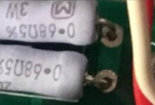
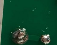
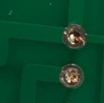
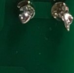
What I see Mosfets and 3W the power resistor soldering joints are not optimal.
Bigger mass, so need heat little more time, or increase the tip temperature.
In this short tutorial You can find instructive, good examples
"Component Soldering"
Attachments
-
 177AF4F4-BC87-444B-91E8-E77751ECBC93.JPG466.1 KB · Views: 193
 -
 E62C33F7-B011-4767-8AC5-430DB098F3F8.JPG476.4 KB · Views: 181
 -
 6F701DD8-D267-42F2-AEBD-FC5F619E7B93.JPG495.3 KB · Views: 323
 -
 F90AA02A-406B-4F15-86AC-2F1370738652.JPG758 KB · Views: 319
 -
 241B9D81-38BA-4834-AA87-30EE88D8E656.JPG560.1 KB · Views: 188
 -
 637A7459-FD44-4BD8-8133-9B7427BF46FF.JPG496.8 KB · Views: 177
 -
 AF760992-81F6-4F39-AEC2-8674A84A901E.JPG590.8 KB · Views: 181
 -
 5CF63FC9-3C94-445B-AD8A-89F2638C7B90.JPG224.1 KB · Views: 143
 -
 5F2299C6-512B-479C-B154-8D106896B433.JPG703.2 KB · Views: 171
I need one of those. I would have thought that I could have gotten it right at least one of those attempts - at least to have corrected the issue. Maybe not with any style points, but still...
Also use the old fashioned solder with 60% tin and 40% lead. It flows much better then the newer Rohs types with no Lead in it. The melting point is lower for 60/40 solder.
Looking at your solder joints it looks like your solder has high melting point.
As one mentioned a solder pump is good to remove old solder and start from fresh with joints that has got too much solder. Get a pump with a soft tip.
The solder has to flow nicely also to the front side for this kind of PCB (e.g. for the pins of the mosfet).
Attachments
Last edited:
Ordered a desoldering pump. Hoping I can get it fixed. Although at this point, I don’t think it is a soldering issue. I’ll resolder in next few days. Hoping it isn’t a lost cause.
Although at this point, I don’t think it is a soldering issue.
Just compare Your solder joints with the good PACE joint example picture 😉
Another tip: always handle with care jfets and mosfets , never touch the metal pins with the fingers beacause electrostatic charge can damage transistors sometimes.
Again compare always with good working channel.
What is Continuity and How to Test for it With a Multimeter
Kind regards 🙂
Attachments
-
 E0149A32-C840-40A2-A0B4-FA7A51F8592B.JPG429.1 KB · Views: 154
 -
 FEEDDE6D-0B54-4F9F-9273-37A20C7365B2.JPG113.8 KB · Views: 395
 -
 62F7BEA6-9A83-400B-80DE-3BFC7430B470.JPG79.4 KB · Views: 398
 -
 DB344C27-0463-4E03-8BDB-CCEE01F3BD04.JPG789.6 KB · Views: 159
 -
 0F94592D-D9BF-4E9D-9543-4DCC03646838.JPG250.2 KB · Views: 158
 -
 637A7459-FD44-4BD8-8133-9B7427BF46FF.JPG496.8 KB · Views: 147
 -
 AF760992-81F6-4F39-AEC2-8674A84A901E.JPG590.8 KB · Views: 123
I must be a soldering issue. If not if makes no sense that you have 16V on one side of R4 and 10V at the other side of R4. R4 is a 0.68 ohm resistor. If you look at the schematic the one side of R4 is same joint where you measure bias voltage at Q1.
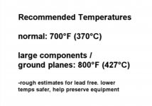
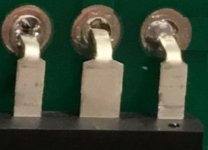
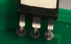
The soldering looks very bad. The temperatur has been too low. Get solder that has approx 180 degree C as melting point and set your iron to 360 - 400 degree C. Then each solder only takes 2 sec. This causes that not much heat will reach the component. Maybe your soldering tip is too thin so it will be cooled down when you hit the joint. For the large joints like mosfets and power resistors you may need a larger tip for your iron that can transfer more heat energy to the joint.
When you solder you also need a wet sponge so you can clean the tip and just apply a tiny bit of solder to the tip so it is just "wet" before each solder. Then it will make good thermal contact to the joint. Then apply solder to finish the soldering. When enough solder is applied and it flows nicely then just keep iron 0.5 sec. at the joint before lifting away fast. It should only take 2 sec. if done right.....maybe 3 sec for the large joints. When you remove the iron and it "pulls" some solder that sticks out from the jont the temperatur is too low. You shall be able to remove the iron from the joint and the joint should still look as the picture above......
Because the whole chassis basically screws together into itself, alignment is a function of every screw you've put into the chassis, all working together in concert.
Make sure the brackets are square on the heatsinks. Loosen the screws that hold the brackets to the faceplate, and the screws that hold the back panel on, attach the bottom plate and use that for alignment, tighten as necessary to keep things square.
Yep, worked just as you suggested. It took some fiddling, but got everything to line up. Thanks!
So, a couple of weeks in and I love this little monster.
One question though, by suggestion I use a 24v brick and set the bias to 12v. It works and sounds beautiful but for my taste it runs a bit hot (a little uncomfortable to touch for more than 5 seconds). What does the higher bias setting do? Does it provide the extra watt people talk about? It does sound like it has a little more ‘oompf’ to it with the 24v brick and higher bias.
Could I lower the bias to 11.5v? What would happen?
Greetz, Dan.
Yes, it gives more power. In a single-ended amplifier you can never pass more current than your bias, so more bias means more power, and more heat.
Lowering the bias would reduce the ultimate power somewhat, though I suspect you won't hear a difference, and lower the heat.
Try 10V to start and see what the heat difference is.
EDIT: Nevermind the heat bit. See below.
Lowering the bias would reduce the ultimate power somewhat, though I suspect you won't hear a difference, and lower the heat.
Try 10V to start and see what the heat difference is.
EDIT: Nevermind the heat bit. See below.
Last edited:
heat is going to be the same , simply because Iq is set fixed in upper half
moving "bias" lower is just transferring more heat to upper mosfet
often we are using term bias as synonym for Iq , but proper use of word is addressing voltage potential , and that can be plenty of things ..... just one of them is commanding a part how much current will go through
moving "bias" lower is just transferring more heat to upper mosfet
often we are using term bias as synonym for Iq , but proper use of word is addressing voltage potential , and that can be plenty of things ..... just one of them is commanding a part how much current will go through
Aha!!
I never noticed that! You are absolutely correct. I was blinded by the simplicity of the pot taking rail voltage to bias the output Mosfet through the Jfet that it didn't dawn on me that it's a divider so what current the output device doesn't get the CCS gets, and vice-versa.
I never noticed that! You are absolutely correct. I was blinded by the simplicity of the pot taking rail voltage to bias the output Mosfet through the Jfet that it didn't dawn on me that it's a divider so what current the output device doesn't get the CCS gets, and vice-versa.
- Status
- Not open for further replies.
- Home
- Amplifiers
- Pass Labs
- ACA V1.5 Illustrated Build Guide