When I adjusted the voltage at R10 to 4.4 the new voltage at Q1 were 0 (left) 15 (middle) 4.5 left
R10 does not seem to be a problem.
Adjust the trimmer so that Q1 middle pin (drain) is 10.5V, same as good channel. What is the Q1 gate voltage (outside pin)? (edited - gate)
Are Q1 and Q2 heating heat up?
What is the voltage drop across R3? (Edited to R3)
Good night.
Adjust the trimmer so that Q1 middle pin (drain) is 10.5V, same as good channel. What is the Q1 gate voltage (outside pin)? (edited - gate)
Are Q1 and Q2 heating heat up?
What is the voltage drop across R3? (Edited to R3)
Good night.
Last edited:
I would just go over the solder connections on both boards.
Many of the connections look questionable.
worked for ten years but corrosion finally caught up.
almost looks like no solder on one of Q3 legs
I cant tell if C4 is swollen or just picture angle.
schematic could help

Many of the connections look questionable.
worked for ten years but corrosion finally caught up.
almost looks like no solder on one of Q3 legs
I cant tell if C4 is swollen or just picture angle.
schematic could help
Last edited:

Well, sorry, I was completely wrong with R10, it was an optical Illusion on my cell phone, I thought the upper side is broken in two parts 🤪
Solder doesn't necessarily need to flow to the top, to make good connection. BUT it is preferable. I'd resolder it again just in case.
almost everything looks like cold solder.
I dont know the board looks hole through pads.
most of it could be touched up from the top.
power connections look cold and blue ground looks corroded.
likely just a connection issue.
schematic would help, dont know looking at current sources or small signal.
only guess current sources are hot all their life. so something may have died.
but it just looks like cold cold solder everywhere
It is a good idea to give the board a good scrubbing with alcohol and a toothbrush. Then check solder joints.
Electrically, the bias voltage to Q1 is adjustable so that is good. Still need to check the voltage drop across R3 to determine current.
Electrically, the bias voltage to Q1 is adjustable so that is good. Still need to check the voltage drop across R3 to determine current.
FYI the heat sink is ice cold so I am thinking this is related to current.
I will scrub, solder and check voltage drop tonight. Time permitting
Question regarding voltage drop. Can you explain how to measure voltage drop?
Earlier you asked for voltage across. So I put my multi meter probs on either side of the resistor should I be measuring between the resistor and the chassis?
As you can see from the soldering I’ve got a lot to learn and appreciate all the help trouble shooting. I’m learning more repairing than when I assembled it way back when. So I guess I’m lucky to have the opportunity to repair it. I’m hopeful we will find a solution.
Thank you!
One side of the resistor to the other side. Since the value of the resistor is known, can compute how much current is flowing (Ohm's Law, V=IxR) given how much voltage the resistor is "scrubbing off". The computed current tells you how much the transistor is conducting.
What did you use for an alternate power supply? And did you isolate the + lead from the existing supply - in case there is something on its output dragging things to a halt?
Yes, measuring voltage drop across a resistor means placing one probe on one side of the resistor and the other probe on the other side of the resistor.
So please measure the voltage drop across R3 and also across R1.
So please measure the voltage drop across R3 and also across R1.
Tjw
I used another laptop charger. The voltage read 20.2 which is what my other charger was reading. One thing to note the charger actually has two hot wires and one neutral. The hots have different voltages. One was around 18 the other 20. It is 19 volt charger
I used another laptop charger. The voltage read 20.2 which is what my other charger was reading. One thing to note the charger actually has two hot wires and one neutral. The hots have different voltages. One was around 18 the other 20. It is 19 volt charger
Ben bellow are the measurements for R1 and R3
Neither Q1 or Q2 is generating any heat
Broken amp
R1 0 volt
R3 0 Volts
Working amp
R1 .25
R3 .35
Neither Q1 or Q2 is generating any heat
Broken amp
R1 0 volt
R3 0 Volts
Working amp
R1 .25
R3 .35
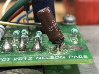
No one noticed C4 is in Backwards ?
I agree it looks swollen too and should be replaced in the correct orientation.
I agree it looks swollen too and should be replaced in the correct orientation.
Indeed it is. It can be removed and can be tested without it for now, unless a replacement is at hand. It may have failed open as voltage was still present and the fuse did not blow. So remove C1 and see if it makes a difference.
As for the R1, R3 voltages at 0V, there was no current flowing, hence the cold mosfets. With no current flowing I am not sure how the voltage at the drain of Q1 was adjustable with adjustment of the trimmer.
Reflow the solder joints and see if that makes a difference. If not, then remove Q2 and Q3 and test them. They may need replacing.
Google "testing NPN transistor with multimeter" and "testing N channel mosfet with multimeter".
Last edited:
Clean the joints with alcohol and toothbrush first.
The solder joints in your image have too much solder. The middle joint does not look like the solder is adhering to the board. So after cleaning the board, put a bit of flux on that joint and reflow. Then see if it works.
- Home
- Amplifiers
- Pass Labs
- ACA failed after a decade Help diagnois