Hi Zen Mod, thanks for the schematic in post 581.
I am sorry, but now I am even more confused:
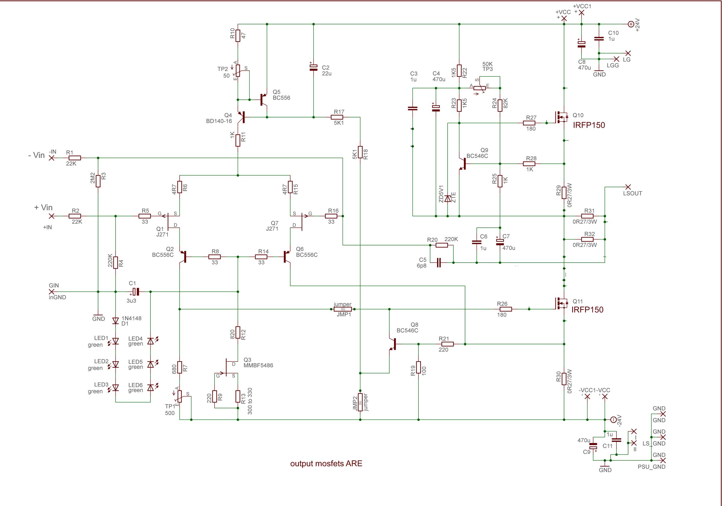
Which version of the schematic corresponds to my PCBs?
I am sorry, but now I am even more confused:
- In the very first post of this thread you indicated that the final schematic and PCB layout is shown in post 138 (11 May 2016).
- The PCBs I received are different from that shown in post 138, so either the layout shown in 138 has been revised since back then, or my PCBs are from an earlier version.
- The schematic you atteched in post 581 is from 30 April 2015.
Which version of the schematic corresponds to my PCBs?
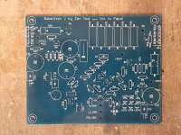
there are no changes , that's sole and final pcb iteration
"additional" resistors - what I already covered in previous posts
"additional" resistors - what I already covered in previous posts
Help me find the problem
Help!
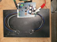
I finished the first board and fired it up. I used a lab / bench PSU set to -20V/0V/+20V, with current limit set to 2A. See photo in the attachment.
The good news is that there was no bang, no magic smoke, and no funny smells; and the green LEDs light up nicely. The bad news is that the speaker out sits at -20V.
I took a good look at the instructions in post #49:
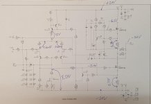
To isolate the problem I took a few voltage readings and noted them in the schematic (attached). As far as I can tell, there is no current flowing though R15, Q7 and Q6.
Any ideas why this would be the case?
Is there a way to check if Q6 or Q7 are okay without taking them out of the PCB?
Any hints and suggestions would be great!
Help!
I finished the first board and fired it up. I used a lab / bench PSU set to -20V/0V/+20V, with current limit set to 2A. See photo in the attachment.
The good news is that there was no bang, no magic smoke, and no funny smells; and the green LEDs light up nicely. The bad news is that the speaker out sits at -20V.
I took a good look at the instructions in post #49:
- I was able to set the LTP current to 10.0 mA using TP2
- I was able to change the idle/bias current of the power MosFETs using TP3
- The speaker output voltage stayed at -20V no matter how much changed TP1, TP2 or TP3
To isolate the problem I took a few voltage readings and noted them in the schematic (attached). As far as I can tell, there is no current flowing though R15, Q7 and Q6.
Any ideas why this would be the case?
Is there a way to check if Q6 or Q7 are okay without taking them out of the PCB?
Any hints and suggestions would be great!
Attachments
Last edited:
mbrennwa,
not answering your question, but I would not dare powering it up with that type of isolation sheet
not answering your question, but I would not dare powering it up with that type of isolation sheet
first thing I'm seeing on pic - never squeeze mosfet with bolt without using proper big washer , plus spring washer ; ceramic case is prone to break if bolted like you did
negative offset means your lower mosfet is having too low impedance - meaning it is too much open
If you don't have any other mistake - check value of R7 and if needed change it to lower value ..... even if I can't fathom how that could be needed - prescribed 5mA per LTP side through 680R ( which is minimal value of R7+TP1 string ) is hardly enough to open lower mosfet to desired value ....... which is approx 4V+ voltage sag across 0R27, ref. to lower rail
ground inputs , both of them , while setting
TP2 is there to be set just once - to have 10V across R11
no easy way of checking Q6 and Q7 without desoldering - but once you did it - bjt is easily check either with diode test or Hfe test in DMM , while JFet is most easily checked with simple JFet matching jig
though , I see no reason that something is gone Puff! , myriad of channels were made , with same equal values and same parts
Help!
.......... I used a lab / bench PSU set to -20V/0V/+20V, with current limit set to 2A. ...........
sometimes that can be tricky part of setup - bench PSU doing his own games
be sure that current limit setting is well above actual needs of circuit
simple variac + regular PSU is much more predictable in behavior
Yep, I mounted the power MosFETs in a quick and very dirty way to the heatsink. This is not the final setup for sure, but it works for now.
Bench PSUs sometimes try to be clever. I am well aware of this and I always make sure that the rail voltages are correct, and that the current limit setting is higher than the real current flowing through the amp. A variac would work well, but I don't have the PSU ready yet.
Ok, here are few more test results:
For some reason Q7 and Q6 don't want to pass current. Both parts are from ZMs bag that came with his PCBs.
Does this ring a bell? Any ideas?
Bench PSUs sometimes try to be clever. I am well aware of this and I always make sure that the rail voltages are correct, and that the current limit setting is higher than the real current flowing through the amp. A variac would work well, but I don't have the PSU ready yet.
Ok, here are few more test results:
- I changed R7 from 680 Ohm to about 400 Ohm. This did the right thing, in the sense that the lower MosFET was now more "closed" than before. I was able to adjust the speaker output to -2V...2V or so, but there was a lot of drift.
- I found that with the lower R7 value the voltage across R15 was still 0 mV, so there was still no current going through Q7 and Q6. I restored R7 to 680 Ohm and then put a jumper across Q6 (collector to emitter), and voila: current was flowing through R15, and adjusting speaker ouput to 0.0 V was possible, with MUCH less drift.
- I desoldered Q6 from the PCB (and damaged the eyelets for Q6 on the PCB in the process). I tested Q6 with the diode tester on my DVM, and it seems fine.
- I found a BC556B in my junk box, so I installed it in the position of Q6 (which should be a BC556C). The amp behaves as with the original BC556C: speaker output sits at -20V, and voltage across R15 is zero.
For some reason Q7 and Q6 don't want to pass current. Both parts are from ZMs bag that came with his PCBs.
Does this ring a bell? Any ideas?
Q6 from bag of my parts is OK with Hfe test , and behaves in circuit same as Q6 from your bag
confirm that you have same voltage at bases of LTP cascodes - Q2 and Q6 , ref to GND
idea is to have them at 6 x LED voltage + PN (1N4148) voltage , which is 6 x 1V93+0V65= -12V2 ( minus means negative , under GND), so emiters are at 0V65 less (-11V55) , and that you need to see at their emiters , thus JFet drains
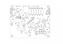
edit: find parts placement pic enclosed , it's handy
confirm that you have same voltage at bases of LTP cascodes - Q2 and Q6 , ref to GND
idea is to have them at 6 x LED voltage + PN (1N4148) voltage , which is 6 x 1V93+0V65= -12V2 ( minus means negative , under GND), so emiters are at 0V65 less (-11V55) , and that you need to see at their emiters , thus JFet drains
edit: find parts placement pic enclosed , it's handy
Attachments
Last edited:
Sucess!
By tracing the voltages around Q6 and Q2 I found a bad solder point. It looked fine, but it wasn't... Thanks for pointing me in the right direction!
Is it okay to leave the BC556B from my junk box in position Q6, or should I put back the BC556C from ZMs bag?
And then there is another thing: during my debugging work I found that the labels of R19 and R21 on the PCB are not consistent with the circuit diagram:
ZM, can you please check this?
Does it make sense to swap the resistors R19 and R21 on the PCB?
In other words, which configuration is correct:
By tracing the voltages around Q6 and Q2 I found a bad solder point. It looked fine, but it wasn't... Thanks for pointing me in the right direction!
Is it okay to leave the BC556B from my junk box in position Q6, or should I put back the BC556C from ZMs bag?
And then there is another thing: during my debugging work I found that the labels of R19 and R21 on the PCB are not consistent with the circuit diagram:
- On the circuit diagram, R19 connects to the negative rail voltage and R21 connects to the source of Q11.
- On the PCB, R19 connects to the source of Q11 and R21 connects to the negative rail voltage.
ZM, can you please check this?
Does it make sense to swap the resistors R19 and R21 on the PCB?
In other words, which configuration is correct:
- 100 Ohm from Q8 to negative rail and 220 Ohm from Q8 to Q11
- 220 Ohm from Q8 to negative rail and 100 Ohm from Q8 to Q11
just remove R19, R21 and Q8
those are parts for Sissies , needing some current limit down
leave your BC in , I don't care much nowadays about supermatching of cascodes
in fact , I don't care of matching them at all
🙂
those are parts for Sissies , needing some current limit down
leave your BC in , I don't care much nowadays about supermatching of cascodes
in fact , I don't care of matching them at all
🙂
just remove R19, R21 and Q8
those are parts for Sissies , needing some current limit down
Ok, now I finally understand what these parts are supposed to do. Why would anyone want to limit the current? Current is good! [emoji6]
Just to say hello from the workshop. Playing beautiful music in test setup with SJEP120R100 (R7 shorted to allow proper adjustment).
ref. to enclosed sch. just value of R7 , decreasing or shortie
Hi ZM
This was your advice when I asked what I need to change in order to use SJEP120R100 instead of IRF150. It works almost fine.
When the amp is cold, the bias current can be adjusted nicely to 2 A. However, once the amp has warmed up, I can't crank up the bias to more than 1.85 A using TP1. I'd like to go to full 2 A (or maybe even slightly higher, as the heatsinks seem to be competent enough). What other changes would be needed to achieve this?
it's easy
if you have P1 in value of 500R , then just increase value of R7 for 500R , whatever value of it you have now
back up with P1 to zero, power up and reset both Iq and DC offset
if you have P1 in value of 500R , then just increase value of R7 for 500R , whatever value of it you have now
back up with P1 to zero, power up and reset both Iq and DC offset
Not so easy... R7 is already a short, as you described in your earlier post regarding the SJEP120R100.
- Home
- Amplifiers
- Pass Labs
- About possible Babelfish J interest