Dear all,
I finished the assembly of my stereo AB100 a few days ago. It runs from an on-board +/50V PSU (600VA Toroidy Audio Grade, active rectification, 2x22mF/rail), and I have cap multipliers instead of the 10R couplings. Q1-Q2-Q4 are 2N5551, Q7 2N5401, Q4-Q5-Q8 KSC3503, Q6 KSA1381. Output stage: Sanken 2SD2390 / 2SB1560, 0R47 emitter resistors (Vishay CPF metal film, 5% 3W 200ppm/C). I use my own pcb layout but it is not very different from those shared by NP or Prasi. Q5, Q6 and Q8 are mounted on the main heatsink, at a ~40mm distance from the nearest Sanken.The small-signal transistors are matched, the output offset is nicely below 3mV. The Sankens are also matched, the variation in the voltage drop on the 0R47 emitter resistors seems to be reasonably small, all 16 values are in the 20-25mV range. I run it over 10 hours, no input and load, with the lid on, checked the voltages on each emitter resistor once in ~30min. After a few iterations of P1, all voltages are beautifully stable, 20-25mV, as mentionned above. Until yesterday night.
The findings of this morning: Same test run as yesterday. Right channel OK. Left channel: PSU voltages are stable (both before and after the cap multipliers), still no offset at the output. The voltage across C12 is 2.4V, not the millivolts are moving anywhere. Yet, what I get is a steadily increasing current on all emitter resistors. In 1-2 minutes they drift from the desired 20-25mV over 200mV, where I turn off the mains for safety. I am puzzled, especially as I did not change anything since yesterday and the right channel still measures everywhere the textbook values.
If you have any suspicions and/or ideas what to test/change please share.
Thanks,
Miklos
A little update: I turned down the output bias and looked out for damages. There seems to be none: R6 and R13 measures 8mA, R11 4mA. Other current levels in the front-end are also normal and stable. Emitter resistors are still around 0R47 and the Sankens are alive, too. Both sides are good. I tend to think that I was simply too daring with the Sanken + 0R47 combination which triggered a thermal runaway at ~50mA bias. So unless you advise otherwise, I will go back to 1R emitter resistors, stay with the Sankens and see again what happens.
Have a nice weekend,
Miklos
Have a nice weekend,
Miklos
Last edited:
I had a thermal runaway on one channel of my build - similar situation as I had my bias a little high and didn’t realize the h/s was slightly blocked in the AV rack. I wasn’t as lucky bc it took out all outputs in my case.
My solution was drop the bias to 15mA (lower by ~50% of where I originally set it, IIRC). That was a couple years ago and no issue since.
My solution was drop the bias to 15mA (lower by ~50% of where I originally set it, IIRC). That was a couple years ago and no issue since.
Thank you for your input, bullitstang. It seems to be in line with my current conclusions.
It was a matter of pure luck that I could prevent actual damages: after I thought I had nicely settled the bias the day before, I plugged in the unloaded amp to an AC power/amp meter, out of curiosity, just to see some power efficiency merits. It started out below 0.5A at 230VAC, as expected, but in a few minutes it reached 2A/230V, a clear sign that something was very wrong. Fortunately I was still standing by and shut down the mains at this point. The 80x300x40 mm heatsink is apparently large enough, it started to 'glow' only with a bit longer delay.
Surely, I have to reduce the bias. At the same time I still think of increasing the emitter resistor values from 0R47 to 1R, following the discussion and the conclusions under this short thread on Class AB biasing:
I do not know if 1R will considerably aid stability while still providing little lower lower distortions with respect to the 0R47 configuration or not but it seems to be safe to expect that it cannot make the stability worse.
It was a matter of pure luck that I could prevent actual damages: after I thought I had nicely settled the bias the day before, I plugged in the unloaded amp to an AC power/amp meter, out of curiosity, just to see some power efficiency merits. It started out below 0.5A at 230VAC, as expected, but in a few minutes it reached 2A/230V, a clear sign that something was very wrong. Fortunately I was still standing by and shut down the mains at this point. The 80x300x40 mm heatsink is apparently large enough, it started to 'glow' only with a bit longer delay.
Surely, I have to reduce the bias. At the same time I still think of increasing the emitter resistor values from 0R47 to 1R, following the discussion and the conclusions under this short thread on Class AB biasing:
Based on the recent discussion, I polished up my simulator and wrote an article summarizing the findings. I think that you will find this to be an easy read and not surprising in outcome.
Class AB Biasing
http://www.edgrochowski.com/articles4/classab.html
Comments are welcome!
Ed
Class AB Biasing
http://www.edgrochowski.com/articles4/classab.html
Comments are welcome!
Ed
- EdGr
- Replies: 62
- Forum: Solid State

I do not know if 1R will considerably aid stability while still providing little lower lower distortions with respect to the 0R47 configuration or not but it seems to be safe to expect that it cannot make the stability worse.
Last edited:
I am using 0.47 emitter resistors as well - but yes, going up to 1r should help with current sharing across each Darlington. Good luck, I think this is a nice sounding amp, and it becomes a better value when you factor in the cost to build (compared to other Class A/B DIY options)
This looks like Q6 isn't reacting nicely when the heatsink heats. I saw in one of the other threads someone had to change the Vbe transistor to get it behave nicely. Since you swapped in a different Vbe transistor, you might want to consider that.
Yes, my very first thought was that something was wrong with the KSC3503 at Q6. But it is alive, it is no farther away from the power devices than in prasi's stable layout, and it has a lot of silicon grease underneath. It does have a similarly higher hFE at higher temperature, just like the variety of the npn's that people typically use in that position. I think the thermal runaway of the Sankens was just too quick and heavy to get it reverted by the temp coefficient of Q6.
Nevertheless, if the Re swap and the reduced, 25-30mA / Darlington bias do not help, I will try some BD139G's from the shelf. I am spoiled, though, by the full plastic TO-126 package of the KSCs, which does not need any additional insulator sheet...
Nevertheless, if the Re swap and the reduced, 25-30mA / Darlington bias do not help, I will try some BD139G's from the shelf. I am spoiled, though, by the full plastic TO-126 package of the KSCs, which does not need any additional insulator sheet...
Looking at the original Pass schematic and layout for the AB100, and at the somewhat modified schematic and layout for Prasi's version, it appears that transistor #8 (Q8) is the component that sets bias for the output transistors. This is the transistor that Nelson says should be located where the heat is, which would be on the main heatsinks. In my build, the output T0-3 Qs will be mounted on angle brackets which are, in turn, bolted to those big heatsinks (with some thermal interface compound in-between to help transmission). Taking my cue from wrenchone (post #1,311), I am planning to use a TTC004B (NPN;T0-126) transistor as Q8. There will be a space on each channel's heatsink between the bracket holding the 4 PNP devices and the bracket holding the 4 NPN devices, which I think is wide enough to screw Q8 directly onto the heat sink that holds both brackets. This seems better than simply mounting Q8 on either bracket alone, which would be closer to some Qs, but which would restrict direct thermal feedback to only one polarity. The wires from the circuit board to the transistor leads would be relatively short. Does this make sense?

All right, not yet finished (speaker protection and hook-up cables are not yet in place) but let there be porn... 🙂


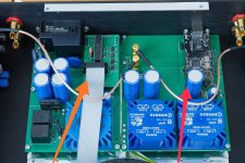
Hi Thimios,
the speaker protection circuit is under optimization, I will share once it is approved. It inspired by Rod Elliot:
https://sound-au.com/project33.htm
but done a bit simpler (less functionality) and all-smd.
What you cite with the arrow is another unit, the atmega board only takes care of slow-start, receiving the IR signals, controlling the volume LEDs, storing volume levels and setting the volume to the dam1121 (which you do not see under the neighbor pcb)
At the beginning I was experimenting a lot with the speaker protection integrated also to the atmega board, so that a full shut-down is also initiated when a dc is detected. But I had so many troubles from false triggerings by turn-on transients, tricks to avoid gnd-loops, etc that after a while I just gave it up. Now it will be enough if the speaker protection boards will be stand alone and only quickly disconnect my precious speakers if needed. I can turn off the amplifier myself when it shall happen.
The USB is an Amanero. It receives the music signal directly from my media center computer and outputs I2S. Underneath there is some galvanic isolation and below the host board is a Soekris dam1121 DAC. The output of the DAC goes directly to the power amps through the SMA cables.
Thanks for answer.
So you have a semi final protection , an R2R dac and a usb to iic pcb inside this amplifier ?
PS you have answer very quickly!
Thanks again.
thimios.
So you have a semi final protection , an R2R dac and a usb to iic pcb inside this amplifier ?
PS you have answer very quickly!
Thanks again.
thimios.
Yes, it is kind of a dac + integrated amp in one chassis (except that there is no conventional pre-amp stage between the dac and the power amp). I still like to call the speaker protection concept "full" but maybe "semi-automated", because it only quickly disconnects the speaker from the faulty power amp but not the entire amp from the mains.
Thank you, Anand! 🙂 I hope it will deserve you compliment when I connect the speakers and press the play button. 🙂Swiss engineering. Beautiful implementation. Take a bow!
Please let us know. I have Prasi’s pcb and I find your implementation of cap multipliers for the small 10 ohm resistor couplings to be creative and intelligent. Other option is to dramatically raise the values of C5, C6 from 100uf to XXX to minimize ripple voltage to the input/driver stages but I do like the idea of small cap multipliers for the same purpose.
Perhaps a small SMD based board to fit right into the 10 ohm resistor holes of R16,R17? If you have a schematic of the cap multipliers to share that would be nice, but I can deduce based on your Eagle pcb layout from post 1523.
Best,
Anand.
Perhaps a small SMD based board to fit right into the 10 ohm resistor holes of R16,R17? If you have a schematic of the cap multipliers to share that would be nice, but I can deduce based on your Eagle pcb layout from post 1523.
Best,
Anand.
- Home
- Amplifiers
- Pass Labs
- AB100 Class AB Power Amplifier