In a word, yes... The total power the heat sink will have to dissipate will be the power per transistor X the total number of transistors. I would advise against getting too frisky with the power dissipation, as this can cause instability.
What are the signs of instability? Do I see it in the stability of the bias itself? It seems very stable but haven't played any music through it. Also then how many class A watts do i have before going into AB. Is it 5W per trannie X total number of trannies in that channel(operation now at 5W per trannie). Heatsink only 37C
On the hole diagrams I've seen there is one green hole that supposedly only exists on the 300 mm deep chassis. What is the hole size for that one? I may consider it for mounting down my Vbe multiplier transistor.
Freecrowder -
Supposedly over-biasing contributes to electrical instability. Depending on the size of your heat sinks. there may also be thermal runaway. At your current bias level of 5W/device (~.125A per device), it looks like you're getting about 0.98W RMS Class A bias per channel.
Supposedly over-biasing contributes to electrical instability. Depending on the size of your heat sinks. there may also be thermal runaway. At your current bias level of 5W/device (~.125A per device), it looks like you're getting about 0.98W RMS Class A bias per channel.
That means I'll need to use a washer stack as a hold-down for my Vbe multiplier - ganky, but serviceable, I guess...
Wrenchone, love that pic BTW, great imagination.
Can you show the math behind the .98W class A. I just guessing but would have thought each device at 5W a piece would have higher class A than that?? I have to say I'm not sure exactly how to calculate.
Can you show the math behind the .98W class A. I just guessing but would have thought each device at 5W a piece would have higher class A than that?? I have to say I'm not sure exactly how to calculate.
BTW I used a crimp on eyelet for VBe. Cut off the plastic insulator on the base where you crimp the wire and open crimp end to insert VBe. Then used needle nose to carfully crimp around VBe and filled with white thermal paste. Then you can bolt directly to HS and seems to work quite well so far.
At 5W/ device (~.125A apiece), you have a total current one one side of 0.5A. That is the total peak current available before you run out of gas and transition to class AB. RMS watts is that peak current X 0.7 squared, times the load impedance (I'm assuming 8 ohms). So, you get 0.5 X .7 = 0.35. That squared is 0.1225. That times 8 ohms is 0.98.

You are not going to get sonic benefits above 100mA from each device.So playing around with the AB100 again on bench. How safe is it to start upping the bias on this amp? I have large heatsinks that are plenty big enough, I have raised from 40mA per transistor to 100mA per transistor. Heatsinks measure at 35 C after an hour there. So what are the limits when doing something like this. So what is the power dissipated in each transistor. Is it voltage across emitter-collector x current through transistor??
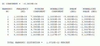
To all punters out there who have actually built this amplifier, what sort of output offset are you seeing? I ran a sim on the current circuit I showed in post 1319 (though I had to sub 2SA965 and 2SC2235 for the VAS drivers and VBE multiplier due to availability of models - they are TO-92L devices similar to the ones used in the original design), and I'm finding it hard to get below around 100mV output offset, and the input diff pair is out of balance. Simulated distortion at 0.2V input (8V output) is around 0.007%, with very low odd-order content, so that's a comfort, at least.
I may need to add an input balance control....
I may need to add an input balance control....
I ran a sim using the Vpulse function of PSpice at the input (10 kHz square wave, 100ns rise/fall, 0.2V amplitude), and as a major consolation prize, the amp appears stable, with no ringing or other monkey business.
Last edited:
I will measure DC offset when I get a chance. My AB100 is used in my garage with garage speakers and it gets heavily abused. I've had it in my garage at least a year.
I just measured mine, built using Prasi's boards with 4 decoupling caps, and I get 7mV on the Left channel and 14 mV on the Right channel. This is cold start offset measurement after setting unused for 4-5 months. After 10 mins pretty stable, went down 1-2 mV on each channel.
Just measured mine, also Prasi boards with 4 decoupling caps. Measured with a Fluke 87III with inputs NOT shorted and nothing connected to outputs. Cold left 2mV right 10mV, hot (left sitting about 2 hours) left -4mV, right -5mV.
I fixed some bonehead **it in my PSpice schematic, also reverting to the original biasing scheme for the diff pair and lower VAS (getting rid of a surface mount part in the bargain). I'm now getting around 1 mV of output offset - no surprise, as the PSpice models for the input diff pair assume identical devices. I'll run a scan when I get back in to work tomorrow to check distortion now that the input diff stage is all nicely balanced out. Yes, I will be matching transistors for the input diff pair and thermally coupling them together when I finally get around to laying out and building this thing.
- Home
- Amplifiers
- Pass Labs
- AB100 Class AB Power Amplifier