
Post#688 where Nelson had answered a similar question.So need opinions. Do people think you could get away with a 200VA trannie on this design? It only being a200 W design
Best,
Anand.
Very underrated amplifier, sounds great, economical - parts and power consumption, safe (if the power supply is lost in one rail...there is no full voltage at the output like in power opamps). There is no switch-on/switch-off thump. Can be scaled down to 30-50w easily,
So while we are at it. Is this design meant to be used with an external cap bank in the power supply or just the one on the boards? I'm using mine with the onboard only and external bridge/XFMR. I have a total of 16400uF per rail/per board. Seems like enough. Any ideas on this.
I think you could go either way. I do like the caps on the board. My opinion, it helps the bass output from this amp.
Or one could put a bank of larger caps offboard , and smaller ones onboard . I'm using the Prasi boards that allow 4x smaller caps or 2x large caps on the board .
Thank you for all your great boards @prasi
Prasi gerbers
https://www.diyaudio.com/community/attachments/stuffing-guide-png.970389/
Thank you for all your great boards @prasi
Prasi gerbers
https://www.diyaudio.com/community/attachments/stuffing-guide-png.970389/
Last edited:
That is what I was meaning fredeb. I have ~33000uF capacitance onboard. Is there any reason to have another bank off board as in conventional PS??
I built mine with 4 caps on the board and a bank off board also. Did it make any difference? No idea. I am happy with it.
I used the the Prasi board with 4-6800uF caps on each board, and I had an off board power supply with 60,000uF per rail, just a little overkill. Dynamics are great.
I decided to do a layout for this board, since I haven't done a purely bipolar amplifier design since around 1977-78. It'll be configured to use currently available devices like KSA992, KSC1845, TTC004B, TTA004B, BSS159, and TIP142 and TIP147. The way I'm biasing the input diff pair and the NPN VAS is a little different as compared to Nelson's original design. I'm also using a bit of degeneration for the input differential stage. I'll use the PCB that I tampered with to make it a lateral fet output design as a template, and strip out what's not needed. I'll use a TTC004B for the bias VBE multiplier, since that will be easy to mount down on the heat sink for bias thermal tracking. I also toned the overall gain down to about 40-ish, so that might get me a little less distortion.
I'm shooting for +/- 40V for the rails. I'll use about 2200uF/rail for local bypassing, and a separate cap bank (using my stash of Apex Jr. 15000uf/63V snap-ins. Schottky rectification is go, using a stash of 150V TO-220FP devices that I grabbed from BG Micro before they folded.
I'm shooting for +/- 40V for the rails. I'll use about 2200uF/rail for local bypassing, and a separate cap bank (using my stash of Apex Jr. 15000uf/63V snap-ins. Schottky rectification is go, using a stash of 150V TO-220FP devices that I grabbed from BG Micro before they folded.
Last edited:
If your Class AB amp resembles the ones that Douglas Self writes about: when driving an 8 ohm load your amp's max voltage at the speaker output will be around (40 - 6) = 34 volts, plus and minus.
Six volts are dropped across the OPS emitter resistors plus the Collector-To-Emitter of the Darlington output transistors plus the collector to rail on the Constant Current Source load of the VAS.
Doing the math, VoutRMS = 34/sqrt(2) = 24.04VRMS --> power into 8 ohms = (24.04) * (24.04) / 8.00 = 72.3 watts.
As long as you don't mind your 100 watt Class AB amplifier having a max power output of 72.3 watts, 40 volt rails are just fine. If you want 100 watts RMS and if you've got a Douglas Self set of voltage drops, plus/minus 46 volt rails will do the job.
I don't mind at all - my living room speakers are vey efficient, and 20W of Class A/side can generate enough volume to run me out of the room. I specifically homed in on 40V rails to give the TIP142s and 147s some breathing room. I may also back off to 0.68 ohms at the output emitters instead of 1 ohm, as I have a bunch of those resistors on hand.
Last edited:
Will your PCB fit the UMS so it will be simple for other builders to build? Would be awesome. 😎
https://cdn.shopify.com/s/files/1/1006/5046/files/universal-mounting-specification-v2.1.pdf
https://cdn.shopify.com/s/files/1/1006/5046/files/universal-mounting-specification-v2.1.pdf
What I see on the attached file is somewhat confusing and doesn't give me much guidance regarding making a board to fit the UMS -my goal would be a board that mounts down completely on the heat sink. I understand that 3mm tapped holes are standard on the heat sink - what is the grid pattern? If don't get enough guidance regarding designing a board to comply with UMS, I will design a board according to my own standards - sorry about that...
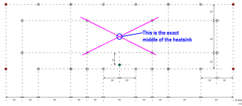
The best place to start for visualization is the 2nd pages which has PCB outlines and device outlines… look at just the green outline and think of that as your best PCB size, as it utilizes the most amount of PCB holes.

The image on the first page has the dimensions/spacings of the M3 holes. The outermost holes, in red, are only on the gigantic 400mm deep chassis and rarely used.

The image on the first page has the dimensions/spacings of the M3 holes. The outermost holes, in red, are only on the gigantic 400mm deep chassis and rarely used.
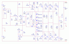
Here's what I have for a preliminary schematic. Q4 will likely be thermally coupled to the Q5 heat sink, using a metal-loaded epoxy like JB Weld or JB Kwik. VBE multiplier transistor Q8 will get mounted on the main heat sink, an easy thing to do as the TTC004B is in a TO-126 full pack. I added some degeneration to the input differential stage, and also reduced the closed-loop gain to ~45. The input electrolytic coupling capacitor was replaced by a film cap - a little more cumbersome, but maybe better-sounding. The two 2200uF caps on the rails are for local bypass. The rest of the energy storage will be via an external cap bank, which likely will also need to conform to the mounting hole pattern on the bottom plate of the std chassis. That may mean that I need to use TO-247 Schottky rectifiers to be able to use an M3 mounting screw. I may go for at least a couple of watts of Class A bias.
Attachments
So playing around with the AB100 again on bench. How safe is it to start upping the bias on this amp? I have large heatsinks that are plenty big enough, I have raised from 40mA per transistor to 100mA per transistor. Heatsinks measure at 35 C after an hour there. So what are the limits when doing something like this. So what is the power dissipated in each transistor. Is it voltage across emitter-collector x current through transistor??
- Home
- Amplifiers
- Pass Labs
- AB100 Class AB Power Amplifier