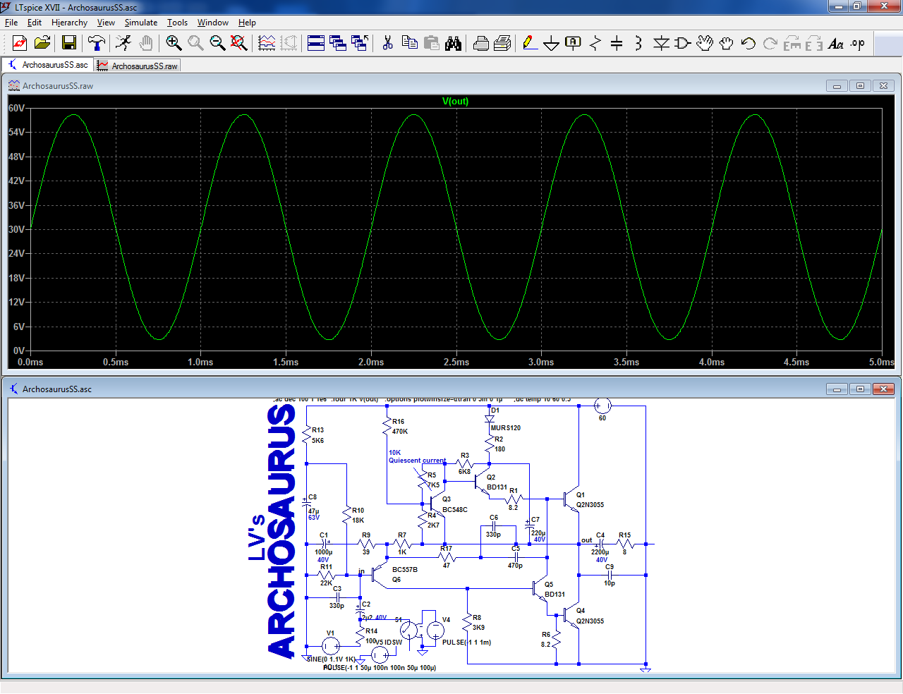
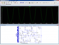
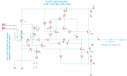
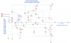
Here is the single supply extrapolation:
Not much has changed, and the performances should remain largely identical.
Note that such a simple circuit will probably suffer from a severe power-on thump; this is difficult to avoid without more complexity.
Given the similarities, Prasi might be able to offer a single PCB design for both versions
Interesting take on the summing of two points for the compensation network. On THD many people subscribe to the First Watt theory and I think it would be useful to investigate this and at other output levels.
That is possible using the .set param command. I have set out the range below 1W in one of these and another for higher powers in another. You can select/deselect by change whichever to comment status.
.step param AV list 0.01V 0.02V 0.03V 0.04V 0.05V 0.06V 0.07V 0.086V
.step param AV list 0.1V 015V 0.2V 025V 0.3V 0.35V 0.4V 0.45V 0.5V
The input voltage is SINE(0 {AV} 1K 0 0 0 16)
The Voltage levels will need to be changed to suit the decrease in closed loop gain recently implemented.
Details for 20k signal tests :
.options maxstep=0.02441555u
.four 20khz 10 4 v(vout)
.option plotwinsize=0
stop time 400us
If the higher harmonics are troublesome beyond 20kHz, preceding the amplifier with Bessel filter stage could have some advantages. You may need a line stage with the reduction in closed loop gain anyway.
The .step param command is useful for other purposes like output loading capacitors. It is not always the larger values that cause problems.
One more proposition: wrt output stage - you can try to sim a really low load (like 1 Ohm or 0.5 Ohm) and optimize the output to be clipped as symmetrically as posible (easier in spice because you are dealing with idealized device parameters; in real life test device variance would "get in the way" of sorts).
I know about the step command, but in this case it is not really useful: the THD is practically completely flat (comprised between 0.45 and 0.65%) for a very large range of output powers.On THD many people subscribe to the First Watt theory and I think it would be useful to investigate this and at other output levels.
That is possible using the .set param command. I have set out the range below 1W in one of these and another for higher powers in another. You can select/deselect by change whichever to comment status.
Such a behavior is quite unusual (and could be useful as a THD-generating test device!) and unnatural, but it is seen in sim only: the real physical thing behaves more consistently, and shows a decreasing THD for decreasing power; at some point (a little under 1W), it passes below the 0.1% threshold.
This, and the fact that the full power THD is already significantly lower than in the sim means that for THD, the sim is unreliable.
It seems reasonably OK for DC, thermal and dynamic conditions, but the linearity has to be tested in reality (and will probably depend on the actual devices used)
The 20K sim will probably be even more meaningless than for 1K, and with an amp having a 30~40K power bandwidth, the 20K THD is probably going to be abysmal, both in sim and reality.Details for 20k signal tests :
.options maxstep=0.02441555u
.four 20khz 10 4 v(vout)
.option plotwinsize=0
stop time 400us
If the higher harmonics are troublesome beyond 20kHz, preceding the amplifier with Bessel filter stage could have some advantages. You may need a line stage with the reduction in closed loop gain anyway.
The .step param command is useful for other purposes like output loading capacitors. It is not always the larger values that cause problems.
This means that in case someone wants to test it anyway, it is not necessary to finesse about the subtleties of timestep: any value will do, and even the .option plotwinsize=0 will make no difference.
This amp is offered for what it is, and it has to be built and measured to be properly evaluated and tweaked.
It has definitely low-performances, but it could be pleasant and tweaked to be so: after all, even its poor performances are sufficient to reproduce most present-day sources without real problem.
In the 60's, 70's, it would even have qualified as HiFi amplifier.
This cannot work with this topology: the gain of the upper part might be lower, but lower half has near-∞ drive capacity, resulting in insane output currents:One more proposition: wrt output stage - you can try to sim a really low load (like 1 Ohm or 0.5 Ohm) and optimize the output to be clipped as symmetrically as posible (easier in spice because you are dealing with idealized device parameters; in real life test device variance would "get in the way" of sorts).
Attachments
At first glance, this circuit resembles the following both (JLH/DOZ)
http://paul-kemble.tripod.com/sound3b.html
Death of Zen - A new Class-A power amp
http://paul-kemble.tripod.com/sound3b.html
Death of Zen - A new Class-A power amp
At first glance, this circuit resembles the following both (JLH/DOZ)
http://paul-kemble.tripod.com/sound3b.html
Death of Zen - A new Class-A power amp
There is a dc adaption of the Rod Elliot circuit at Death of Zen 15 watt Power Amplifier
Here is the single supply extrapolation:
Given the similarities, Prasi might be able to offer a single PCB design for both versions
Sure, Elvee,
I will start working on it.
regards
Prasi
Yes, at first glance: they are both totem-pole and look very similar, however there is an essential difference: the JLH is designed for class A, and the Archo for class AB.At first glance, this circuit resembles the following both (JLH/DOZ)
If you tried to reduce the bias of a JLH to AB level, it would cease to work properly: it would operate for a small class A range, and then clip.
If you push the Archo into class A, it will continue to function, but its performances are not going to match a JLH.
To make a "proper" AB starting from a JLH, you would normally need to reduce the emitter resistors, to 8.2 ohm for example, and use a bias current about twice as large as for the JLH, because at any time, half of the bias will be wasted in the base-emitter resistors.
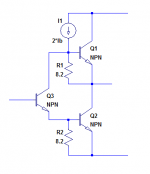
Conceptually, it would look like this.
Of course, a substantial amount of power will be lost by the the bias, which is why I tampered with this scheme: the transistors I added shift the threshold of the upper half by ~1Vbe, meaning that the bias current only needs to be slightly larger than Ib.
Benefits don't stop there: thanks to the bootstrap which is now possible and to the amplifier transistor, the positive swing is increased, and the available peak drive current is larger for both halves.
Thus with a lower dissipation, the circuit allows a larger output power and also allows a good thermal compensation.
The cost is that the PP is now lopsided, and the virtual complementarity is somewhat damaged...
It would probably be possible to use some of the Archo trick in an improved JLH, to make the standing current more deterministic (it is currently defined by the transistor's Hfe) and more stable
Attachments
What happens if you connect Q2 C directly to D1 K? You could also try to make the R3 6K8 resistor a bit smaller value.This cannot work with this topology: the gain of the upper part might be lower, but lower half has near-∞ drive capacity, resulting in insane output currents:
Here it is:What happens if you connect Q2 C directly to D1 K?
R3 halved:You could also try to make the R3 6K8 resistor a bit smaller value.
Attachments
Baby steps (what is the improvement? one Ampere better upper-drive?) ... if you drop the R1 value a tiny bit (say 6.8 Ohm) the upper-halve's drive will get yet a liiiiiittle better.
But does it matter?
(hmm and it rhymes ...)
But does it matter?
(hmm and it rhymes ...)
Hello Elvee,
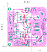
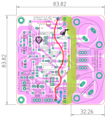
Here is the dual rail PCB adapted for single rail.
Please let me know if its ok? Then I will post pdf and gerbers.
adaptations for single rail are shown in blue color both on sch and layout.
regards
prasi
Here is the dual rail PCB adapted for single rail.
Please let me know if its ok? Then I will post pdf and gerbers.
adaptations for single rail are shown in blue color both on sch and layout.
regards
prasi
Attachments
Last edited:
I don't think so: this is a dinosaur having resisted changes for eons, and it will continue to do so...But does it matter?
Builders have to accept it as it is, or opt for something more evolved
Excellent work, it looks OK.Hello Elvee,
Here is the dual rail PCB adapted for single rail.
Please let me know if its ok? Then I will post pdf and gerbers.
adaptations for single rail are shown in blue color both on sch and layout.
Of course, I remind would-be builders that it remains somewhat experimental: even with a correct layout, depending on the components, your mileage may vary (but any issue should be fixable)
With regard to biasing T2 it is usual convention to make R9 a fixed value and R8 the variable adjustment. There is a reason for that.
Hello all,
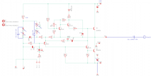
here is the final design, unless someone have any observations.
I have also exchanged positions of R9/R8.
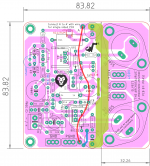
I have the pdfs, sch, stuffing guide and gerbers.
Build notes:
1. Information in blue indicates the changes required for single rail version in the sch and layout.
2. PCB is double sided. If single sided PCB is done, then jumper J1 and wire from A' to A' is required.
3. T2 is mounted from bottom side and stuck to the heatsink Aluminium angle.
4. Drill out the aluminium angle material below the faston connectors of +/out/-.
5. D4 is SMD and mounted from bottom side.
6. Finally, All the best for build..🙂
regards
Prasi
here is the final design, unless someone have any observations.
I have also exchanged positions of R9/R8.
I have the pdfs, sch, stuffing guide and gerbers.
Build notes:
1. Information in blue indicates the changes required for single rail version in the sch and layout.
2. PCB is double sided. If single sided PCB is done, then jumper J1 and wire from A' to A' is required.
3. T2 is mounted from bottom side and stuck to the heatsink Aluminium angle.
4. Drill out the aluminium angle material below the faston connectors of +/out/-.
5. D4 is SMD and mounted from bottom side.
6. Finally, All the best for build..🙂
regards
Prasi
Attachments

Last edited:
Yes but when making R8 variable, an additional end resistor should be added because there is something worse than a wiper losing the track: a trimmer fully turned to the zero-ohm end stop.With regard to biasing T2 it is usual convention to make R9 a fixed value and R8 the variable adjustment. There is a reason for that.
If that option is retained, R9 should be for example 2K2 variable + 1K5 fixed, and R8 6K8 fixed.
Not a high priority mod
Yes but when making R8 variable, an additional end resistor should be added because there is something worse than a wiper losing the track: a trimmer fully turned to the zero-ohm end stop.
If that option is retained, R9 should be for example 2K2 variable + 1K5 fixed, and R8 6K8 fixed.
Not a high priority mod
Agreed, the risk is that a trim pot is a mechanical part. If the contact of the adjustment is compromised the output transistor standing current will reduce. That reduces the possibility of failures if someone drops a screwdriver into the works while tinkering - allowances for people that is.
Yes but when making R8 variable, an additional end resistor should be added because there is something worse than a wiper losing the track: a trimmer fully turned to the zero-ohm end stop.
If that option is retained, R9 should be for example 2K2 variable + 1K5 fixed, and R8 6K8 fixed.
Not a high priority mod
Like this?
Attachments

Hello all,
here is the final design, unless someone have any observations.
I have also exchanged positions of R9/R8.
I have the pdfs, sch, stuffing guide and gerbers.
Build notes:
1. Information in blue indicates the changes required for single rail version in the sch and layout.
2. PCB is double sided. If single sided PCB is done, then jumper J1 and wire from A' to A' is required.
3. T2 is mounted from bottom side and stuck to the heatsink Aluminium angle.
4. Drill out the aluminium angle material below the faston connectors of +/out/-.
5. D4 is SMD and mounted from bottom side.
6. Finally, All the best for build..🙂
regards
Prasi
Here is version R3 with split resistors for T2 as discussed in few posts above.
Attachments
- Home
- Amplifiers
- Solid State
- A prehistoric amplifier: The Archosaurus