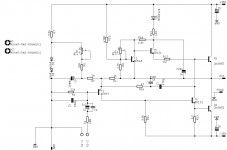
I used a opamp for simplicity only; it auto-centers the DC bias and simplifies the sim a lot because the focus should be on optimizing the output totem solely...
My conclusion was the whole upper/lower totem simmetry and drive is the issue that needs some polish; but it can be done within the already established circuit.
My conclusion was the whole upper/lower totem simmetry and drive is the issue that needs some polish; but it can be done within the already established circuit.
Using a BD139 in the initial circuit does markedly improve the slew performances, but not as much as with pure class A
That was one of my first ideas, because R1 is in series with the dynamic emitter resistance of Q2, and to restore symmetry, it should be made lower (and one of the sims I posted earlier uses a smaller resistor) , but the tests I made do not seem very conclusive. The issue remains open.
Using an opamp in this circuit is definitely off-limits for me, but feel free to post any variation on the theme, even if it looks somewhat extravagant: some people (including myself) could be interested
I have the same message for Mjona: don't fear to hijack the thread in this way.
... and since this thread is not an actual project (yet), just a basic framework, any positive contribution is welcome.
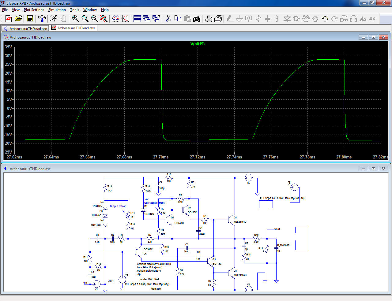
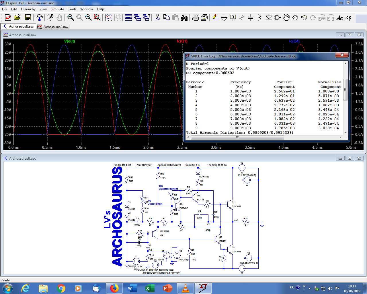
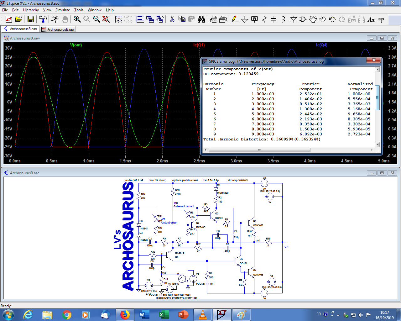
Thanks for posting your .asc file. I have not solved the enigma but I have tinkered with this a bit and the best THD result for 1kHz sine with roughly 22V peak output is 0.2%.
I substituted Cordell .models in combination with some in the SPICE library.
The main change I made was after using the visible traces tool to check the current passing through C1. This gets up over 81 m.A. and should have resembled the negative swing of the sine wave input.
I attributed that it did not do so owing to the presence of the diode in series with R3 which I increased in value to 270R and deleted the diode.
This improved the THD % but only slightly. The I(C1) shape changed for the better but it could do with some more work. I will attach some images to a later post.
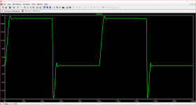
I noticed the sine wave out up and down peak levels wobble a bit at the start. These peaks settle to be even by the fourth cycle after 3.73 ms.
Resolving that is not as simple as fitting BD139's and MJL21194's.
The area to consider is the compound transistor arrangement with Q3 and Q2. The visible trace tool can be used to look at Ic shapes and the respective time bases.
The output of Q3 and Q2 is inverted so in series the output at the end of this chain ought to be the same as the input.
The aim here is perhaps to have that mostly so with some delicate mismatch in contour to limit the output standing current to avoid running in Class A.
Miller capacitance in common emitter amplifiers reduces frequency response which has an inverse relationship with time. To further complicate matters there is ac feedback through the "bootstrap" capacitor.
As you don't mention it explicitly, I hope you didn't use the "-sw" version for normal, sinewave testing (it is for step tests only).
If you did, you are going to see oddities because, of the reduced values of the caps
If you did, you are going to see oddities because, of the reduced values of the caps
As you don't mention it explicitly, I hope you didn't use the "-sw" version for normal, sinewave testing (it is for step tests only).
If you did, you are going to see oddities because, of the reduced values of the caps
I missed the change to the value of the feedback to earth decoupling cap which you had at 4700uF in the first version of your circuit.
Thanks for pointing to the oversight. Correcting this corrects the time alignment and the wave pattern along with that.
The bootstrap cap was optimum at 220uF - I did try some other values.
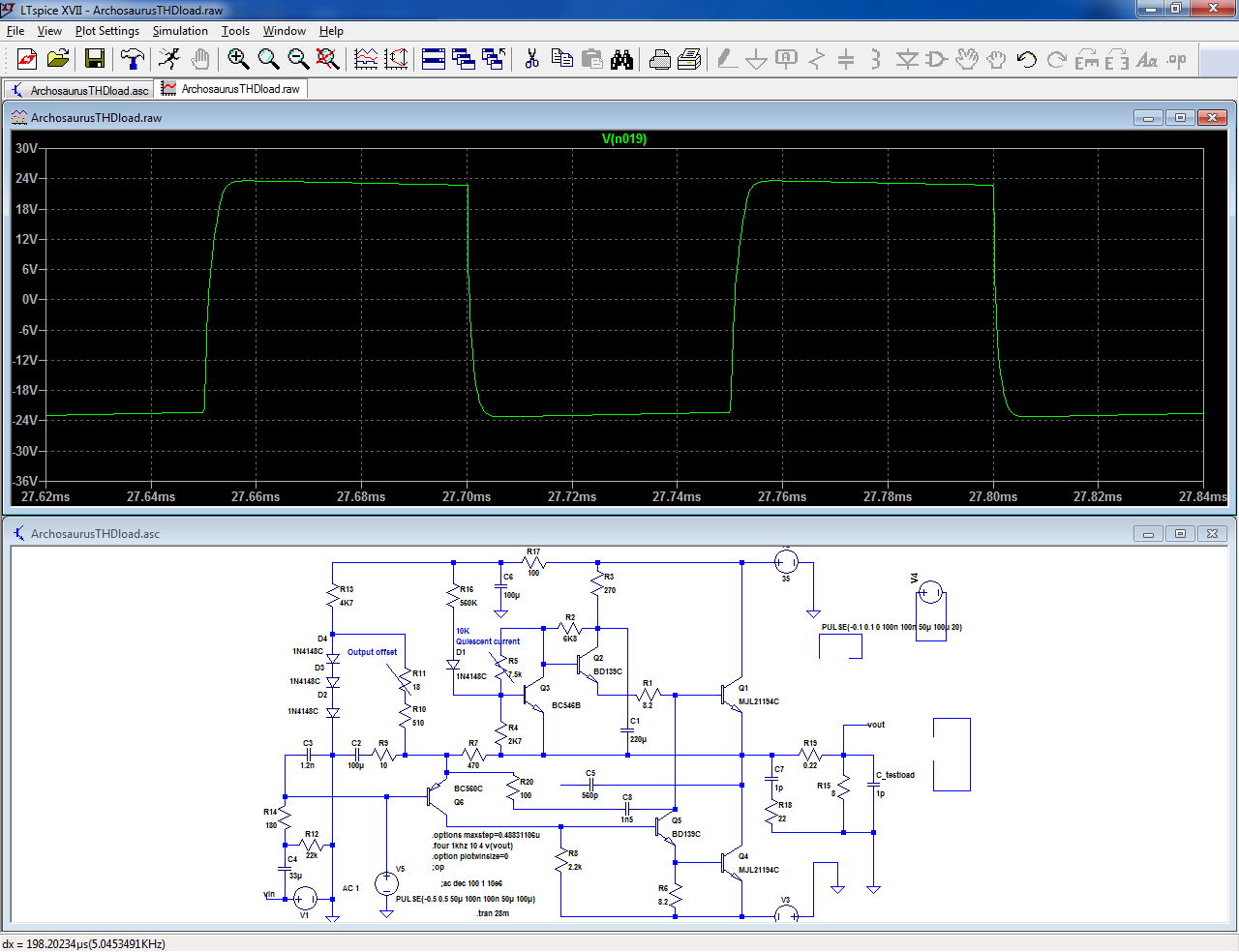
The standing current for the output stage in my simulation was over 120 m.A. with BD139 and MJL21194.
I have reinstated the diode 220R resistor combination and reduced the output standing current to 54 m.A. which makes a small reduction in 1kHz THD to .18% on paper. It should run cooler as a result.
I found that the lowest distortion does not guarantee the most uniform picture of the harmonics in the FFT so at 1kHz audibly speaking some higher order ones might stick out.
Last edited:
My goal in this would be minimizing the # of wires to build point to point. Not using up historic RCA transistors that I didn't buy in 1974 because I was too poor. IC amp LM1875 point to point was a big failure: Motorboated. Wires too long probably.I used a opamp for simplicity only; it auto-centers the DC bias and simplifies the sim a lot because the focus should be on optimizing the output totem solely...
If I build this, to prevent from burning a $600 speaker, I'd leave out the transformer center tap connection. So to auto center the former center tap line I'd use an LM675 TO-220 60 v capable op amp.
Last edited:
My goal in this would be minimizing the # of wires to build point to point. Not using up historic RCA transistors that I didn't buy in 1974 because I was too poor.
The local stockist here has 2N3773 available over the counter. The ones made by RCA were Homextial base types according to my 1978 RCA Handbook.
Those in the Motorola 1984 Selector Guide have an fT of 4MHz which suggests these are Epitaxial base. Both versions are rated for 16 A and 150W with Vceo of 140V.
I used Motorola 2N3773 for a quasi-complementary amplifier back around 1980 - these came in an alloy TO-3 case.
I missed the change to the value of the feedback to earth decoupling cap which you had at 4700uF in the first version of your circuit.
Thanks for pointing to the oversight. Correcting this corrects the time alignment and the wave pattern along with that.
The bootstrap cap was optimum at 220uF - I did try some other values.
The standing current for the output stage in my simulation was over 120 m.A. with BD139 and MJL21194.
I have reinstated the diode 220R resistor combination and reduced the output standing current to 54 m.A. which makes a small reduction in 1kHz THD to .18% on paper. It should run cooler as a result.
I found that the lowest distortion does not guarantee the most uniform picture of the harmonics in the FFT so at 1kHz audibly speaking some higher order ones might stick out.
Following on from this I found in the simulation the circuit would not tolerate a capacitor in parallel with the load and so I did some more investigation so it would handle 1u in parallel with 8R.
The emitters of Q3 and Q1 connect to the output line so if the voltage at that point changes as it will with ac then that will impact on the base voltage for both transistors at the same time.
The chain Q3, Q2, and Q1 are driven by that voltage so when the output voltage moves toward the positive rail it will push back against the drive due to R16 (560R) biasing the base of Q3.
We have D1 in the collector of Q2 the intermediate part of the chain - it would do better in series with R16 at the bias entry point. The idea was to provide some resilience as happens when a tennis ball is squeezed and released.
I made some other detail changes 1. RC decoupling of the positive supply 2. buffering the output to prevent out of phase signals upsetting the nfb 3. added a zobel at the output 4. Increased the input load resistor to ease the drive requirement.
The THD has regressed slightly but this is not too bad with a 1uF test capacitor parallel with 8R
Attachments
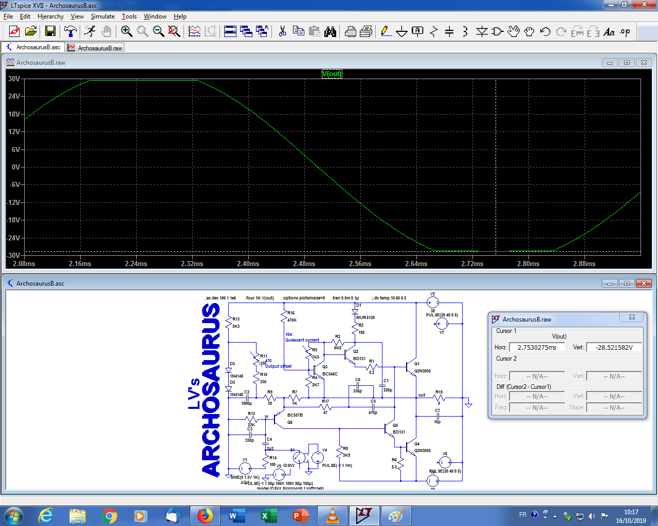
THe mods do provide some improvement on some aspects, but unfortunately they also completely ruin the large signal step response: even with a BD139 as phase-splitter, the slew asymmetry is degraded compared to the original circuit with a TIP41.
This is obviously caused by the OIC: when the comp is restored to the input-inclusive original, normality is restored.
(I removed the output caps for the tests, as they degrade the waveforms even more)
This is obviously caused by the OIC: when the comp is restored to the input-inclusive original, normality is restored.
(I removed the output caps for the tests, as they degrade the waveforms even more)
Attachments
Hello Elvee,
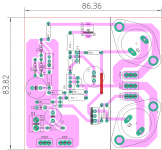
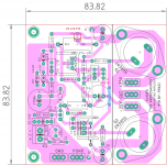
Here is a rough layout.
Can you tell me if its ok? and also any resistors of high wattage, other than regular 0.25W.
C3 /C4 are 13mm dia caps. Can you tell me the voltage requirement of these caps?, so I can place appropriate cap sizes.
regards
Prasi
Here is a rough layout.
Can you tell me if its ok? and also any resistors of high wattage, other than regular 0.25W.
C3 /C4 are 13mm dia caps. Can you tell me the voltage requirement of these caps?, so I can place appropriate cap sizes.
regards
Prasi
Attachments

HARE KRISHNA PRASI
- (In your schem) R4-R11-R12 will need be of higher rating (I suppose around 2W)
- I would also swap the positions of R8 and R9 (a bit dangerous imo)
BUT WAIT for the author to officialy declare the circuit to be "approved"!
- (In your schem) R4-R11-R12 will need be of higher rating (I suppose around 2W)
- I would also swap the positions of R8 and R9 (a bit dangerous imo)
BUT WAIT for the author to officialy declare the circuit to be "approved"!
Hare Krishna!... Anti,
Thank you for your comments.
Yes, I will definately wait for author's comments before posting pdf and gerbers.
Meanwhile here is slightly improved , including some of your comments (except swap of R8 and R9).
regards
Prasi
PS.
(Have you been to ISKCON some time ?🙂
Thank you for your comments.
Yes, I will definately wait for author's comments before posting pdf and gerbers.
Meanwhile here is slightly improved , including some of your comments (except swap of R8 and R9).
regards
Prasi
PS.
(Have you been to ISKCON some time ?🙂
Attachments

Last edited:
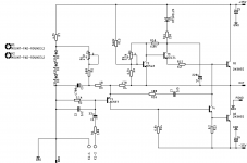
Here are some preliminary comments, but be aware that the circuit is a provisional study work, not intended for actual use.
Thus, ideally some changes will be required, but they will mostly affect parameters like gain (which is currently too high) and just require components value changes, not the basic circuit.
For up to 40V supplies, R11 should be 5W, and it looks OK (depends on the type: some are more compact than others).
R4 will have a larger value, so 1W is OK.
R12 can be 0.25W
C4 needs a little more than the max supply, so 50V should be fine
C2 can be 3V, but its value will be reduced
C1 can be 16V, and its value will also be reduced
R1 is optional, but it can be left in place: it could also be a ferrite bead
T4 is certainly not going to be a TIP41, because of its poor performance, it will rather be a TO126, but no change is required and the heatsink will even have a better orientation
Local supply bypass caps could be included, more as a precaution and to avoid disturbing other audio blocks with the supply wiring than as a real necessity for the amplifier itself, because its topology will make it mostly immune to supply impedance, but it is good practice anyway.
47µF/50V should do.
And finally, the most important (and probably the most problematic for the layout): T2 should be in close thermal contact with the main heatsink
Something not present in the original schematic is the bias compensating resistor R16, which is going to be useful for different builds and could therefore already be included:
Don't hurry too much finalizing the design: there might still be some changes here and there, and I am going to propose a single supply version for Indianajo, and since the changes should be very minor, it could be possible to accommodate both versions with a single PCB
Attachments
THe mods do provide some improvement on some aspects, but unfortunately they also completely ruin the large signal step response: even with a BD139 as phase-splitter, the slew asymmetry is degraded compared to the original circuit with a TIP41.
For the same signal input level the BD139 gives a peak voltage that is about 3V greater than the TIP41C.
Both of these devices result in square wave shapes than indicate loss of gain which shows up worse with the latter.
The loss of gain does not necessarily indicate in stability in fact the circuit has some level of in-built compensation with the TIP whose fT is given as 3MHz.
The datasheets for MJL21194C give fT as 6MHz for current from 100 m.A. up to 5A.
The original devices are RCA 2N3055 so with this, in no way would the unaided TIP41C act as the dominant pole.
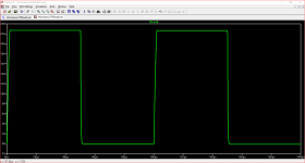
The attached images show square wave with no compensation at all. This is into 8R only.
Attachments
Thank you Elvee for your comments.
I will do mods as and when its being finalized and design is frozen.
Meanwhile, here is a layout that takes care of all your comments.
T2 is mounted from bottom side and can be stuck to the aluminium angle on which output devices are mounted.
A' to A' is connected by an insulated wire from bottom (Light grey line).
regards
Prasi
Attachments
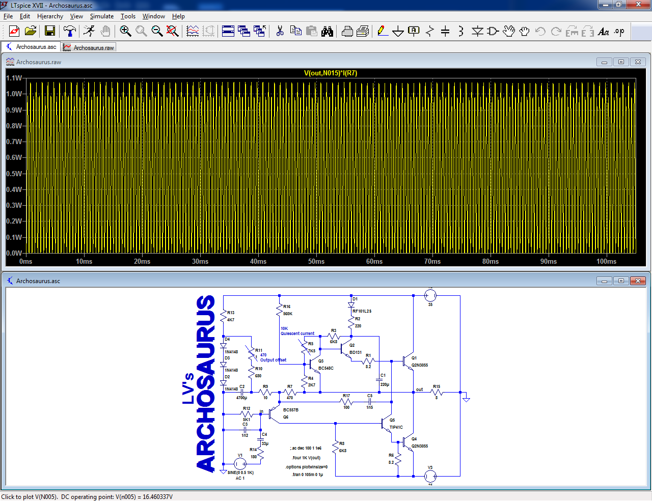
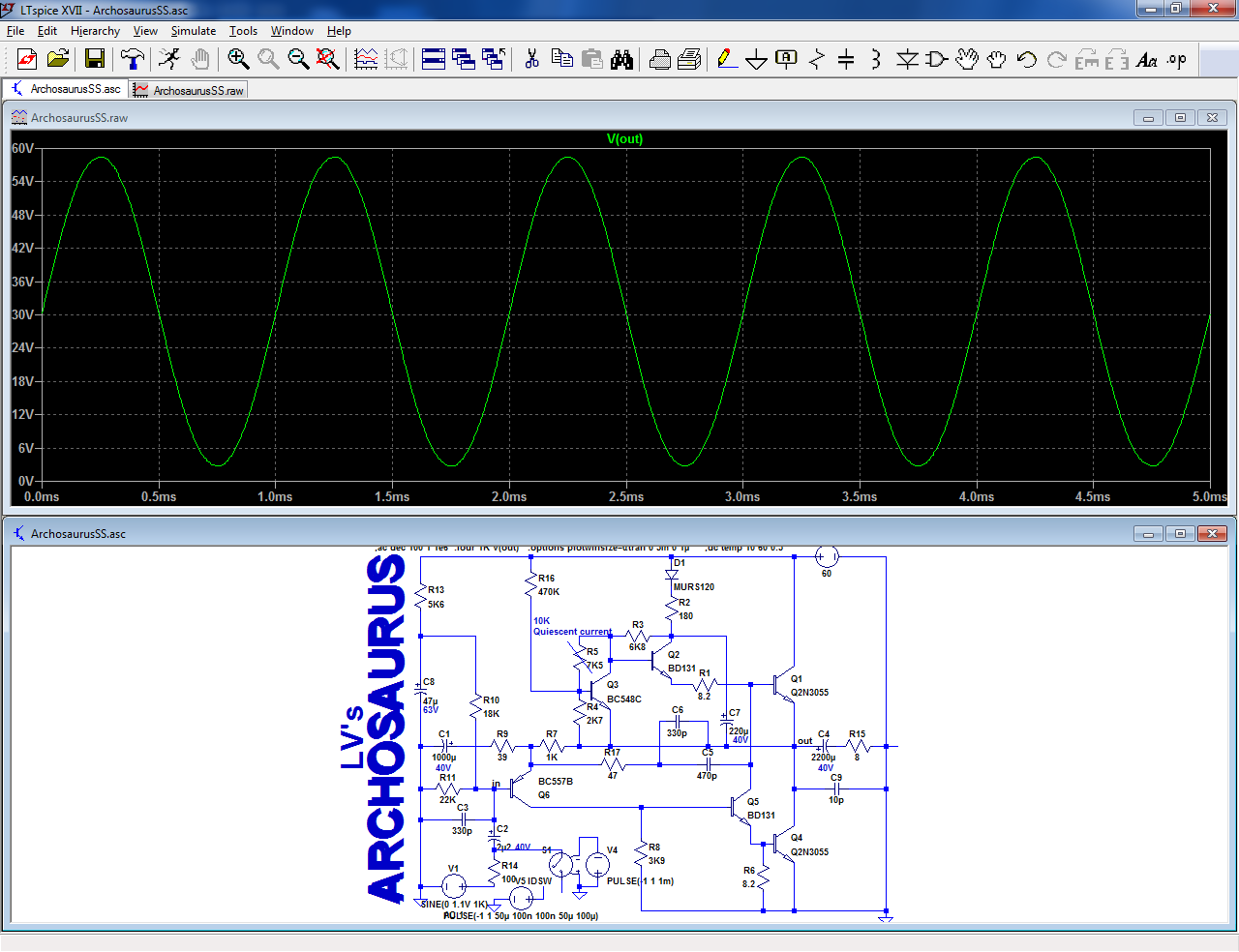
Here is the smoothed out version of this project. Mind you, it remains extremely crude and rudimentary, in a word prehistoric, but it has some redeeming features.
The supply voltage is now centered on 30V nominal, and the sensitivity 700mV rms: both are more reasonable.
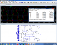
The full power THD is 0.6%, which is a bit surprising, but the actual THD will probably be somewhat lower, as in my prototype:
Interestingly, the THD is mainly H2, indicating an asymmetry between the top and bottom parts of the PP.
The higher part has a higher gain, and this can be fixed by inserting a small resistor in the emitter:
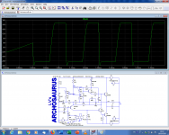
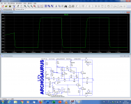
Here is the clipping behavior:
It is clean, and arrives within <1.5V of the rails, so not too bad.
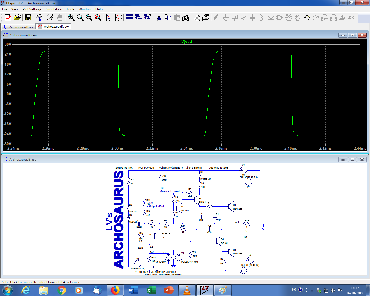
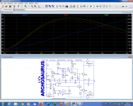
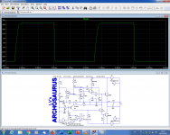
Here is the large signal step response, first on resistive load:

On a 100n capacitive load:
It is still acceptable with 1µF:
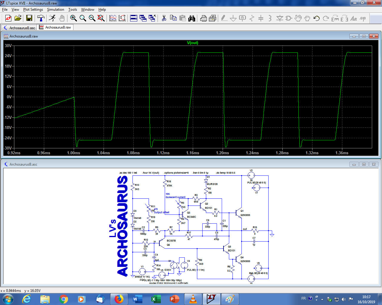
And even with a pure 1µF:
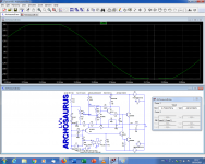
Here is the Iq evolution with supply voltage:
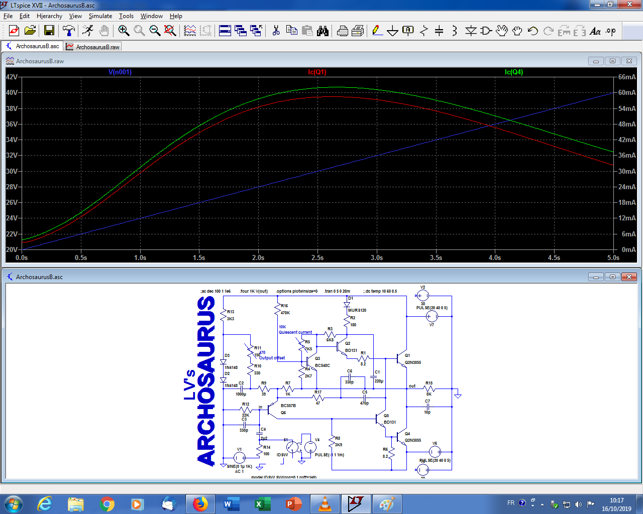
With temperature:
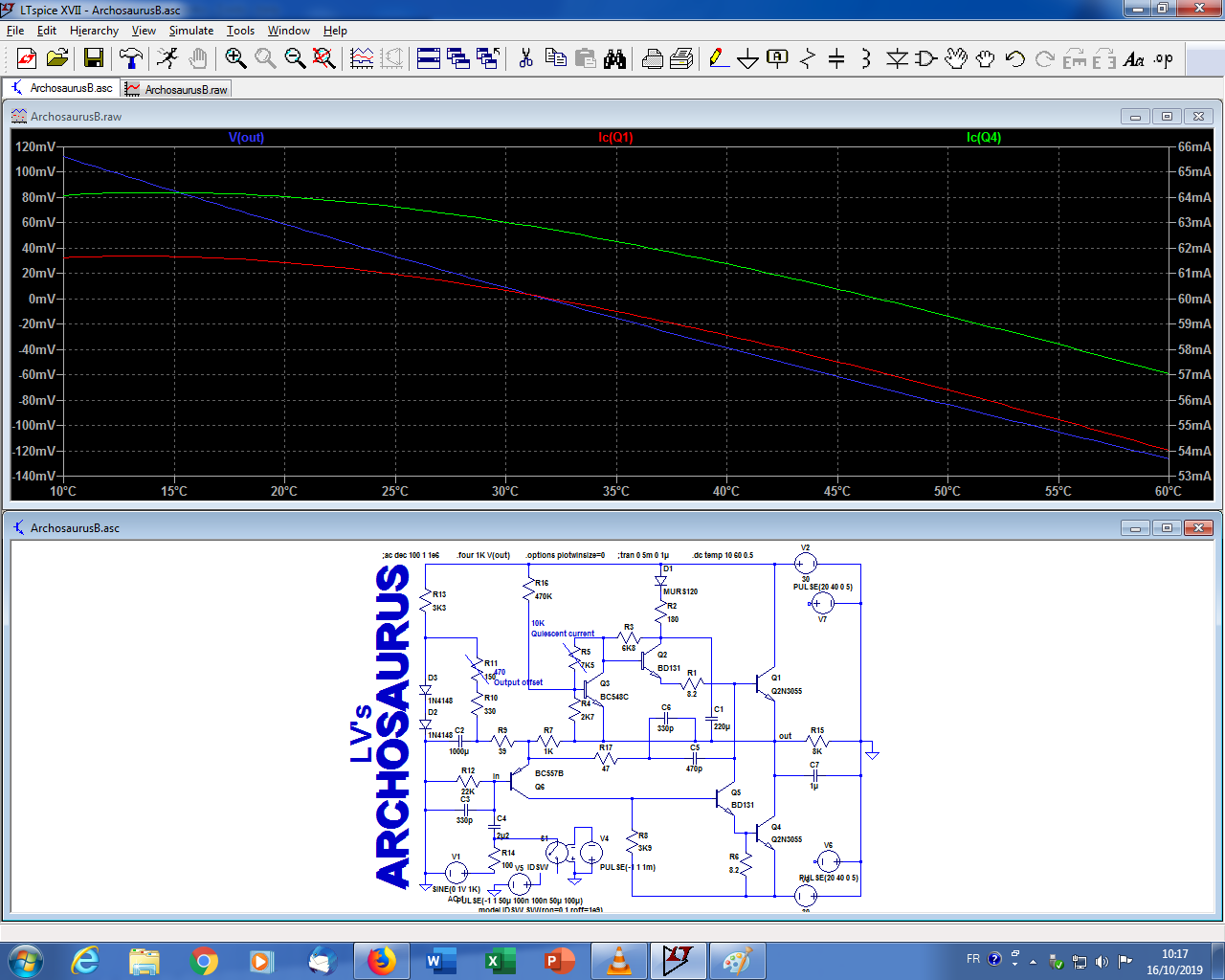
It has a moderate negative tempco, but the sim assumes uniform temperature changes, which is not going to be the case in the real world, even if all devices are on the same sink.
The tempco would become positive, but with Prasi's implementation, the tempco will become negative because Q2 has a separate heatsink.
I didn't include a filter for the + supply, not that it does not improve the PSRR, but the negative PSRR is even worse, and nothing can be done (simply) there, so we have to live with it: after all this is the Archosaurus, the prehistoric amplifier....
I await remarks and suggestions
The supply voltage is now centered on 30V nominal, and the sensitivity 700mV rms: both are more reasonable.
The full power THD is 0.6%, which is a bit surprising, but the actual THD will probably be somewhat lower, as in my prototype:
Interestingly, the THD is mainly H2, indicating an asymmetry between the top and bottom parts of the PP.
The higher part has a higher gain, and this can be fixed by inserting a small resistor in the emitter:
Here is the clipping behavior:
It is clean, and arrives within <1.5V of the rails, so not too bad.
Here is the large signal step response, first on resistive load:
On a 100n capacitive load:
It is still acceptable with 1µF:
And even with a pure 1µF:
Here is the Iq evolution with supply voltage:
With temperature:
It has a moderate negative tempco, but the sim assumes uniform temperature changes, which is not going to be the case in the real world, even if all devices are on the same sink.
The tempco would become positive, but with Prasi's implementation, the tempco will become negative because Q2 has a separate heatsink.
I didn't include a filter for the + supply, not that it does not improve the PSRR, but the negative PSRR is even worse, and nothing can be done (simply) there, so we have to live with it: after all this is the Archosaurus, the prehistoric amplifier....
I await remarks and suggestions
Attachments
-
ArchosaurusB.asc7 KB · Views: 84
-
 ArchosaurusB7.png125.3 KB · Views: 371
 -
 ArchosaurusB8.png125.9 KB · Views: 381
 -
 ArchosaurusB6.png140.1 KB · Views: 381
 -
 ArchosaurusB5.png116.1 KB · Views: 374
 -
 ArchosaurusB4.png140 KB · Views: 362
 -
 ArchosaurusB3.png131.3 KB · Views: 364
 -
 ArchosaurusB2.png169.8 KB · Views: 370
 -
 ArchosaurusB1.png176.1 KB · Views: 370
Tempted to do a build based on this for a small subwoofer, as I think I can find suitable parts in the junk bin. Maybe even in the same dead-bug style just to keep it simple.
One question - D1 appears to be a fast recovery type, not something I have on hand. Does it matter very much what type of diode is used here?
One question - D1 appears to be a fast recovery type, not something I have on hand. Does it matter very much what type of diode is used here?

Here is the smoothed out version of this project. Mind you, it remains extremely crude and rudimentary, in a word prehistoric, but it has some redeeming features.
The supply voltage is now centered on 30V nominal, and the sensitivity 700mV rms: both are more reasonable.
The full power THD is 0.6%, which is a bit surprising, but the actual THD will probably be somewhat lower, as in my prototype:
I await remarks and suggestions
I notice the value of R15 in your .asc is "8K" rather than 8R.
Be aware that the performances aren't particularly stunning, but for subwoofer use, a 30~40kHz power bandwidth should be sufficient.Tempted to do a build based on this for a small subwoofer, as I think I can find suitable parts in the junk bin. Maybe even in the same dead-bug style just to keep it simple.
Note that two other simple amplifiers I have described earlier offer significantly better performances for a similar level of complexity: EZmos and Old-Fashioned 1 (but they require a little more than mere 2N3055's).
Also note that the PSRR is relatively poor.
If your supply has sufficient filter caps, this shouldn't be an issue, unless you have extra-sensitive speakers.
With normal speakers and good supply caps, no hum should be noticeable if you bias the amplifiers at a few tens of mA.
The diode should preferably be fast, and a 1N4148 should have just enough current to be suitable, but a slightly larger one like BAX16, BAV20, etc would be better.One question - D1 appears to be a fast recovery type, not something I have on hand. Does it matter very much what type of diode is used here?
In fact, even a slow diode will work, because it will only switch at very high power levels, when the THD approaches 0.5%, so it will make no practical difference.
You could even omit it: the result will be a slightly warmer R2, and a marginally reduced drive for the OP's, but it will work without.
Looks fine, now I am going to work on the single supply versionSims looking nice and should be good to go...🙂
Here is the single supply extrapolation:
Not much has changed, and the performances should remain largely identical.
Note that such a simple circuit will probably suffer from a severe power-on thump; this is difficult to avoid without more complexity.
Given the similarities, Prasi might be able to offer a single PCB design for both versions
Attachments
Last edited:
- Home
- Amplifiers
- Solid State
- A prehistoric amplifier: The Archosaurus