Well, this design is taken from the Figure 14.17 of the book "Designing Audio Power Amplifiers" by Bob Cordell. I took it like this without deep thinking but, referring back to the paragraph of the book about the Bias Spreader and Output Stage, page 346, I quote:A related question - why the two transistor CFP bias spreader for Lateral FETs? Most designs with Laterals use a simple resistor biasing network since Laterals have a positive tempco. They typically don't need anything fancy.
The bias spreader is a CFP design hat typically supplies a spread of about 2.7 V to bias the output lateral MOSFETs and their BJT emitter follower drivers. The CFP bias spreader provides a stiff, low-impedance voltage drop that is advantageous for full complementary designs like this, wherein the VAS bias current can be somewhat more variable than in single-ended designs where the VAS bias current is set by a fixed current source.
Again, from the book, page 332, and I quote:does it make more sense to but [put] also the bias spreader on the heatsink....?? with another type of bjt´s of course
Because TCvgs for lateral MOSFET is approximately zero at the quiescent bias level, the traditional Vbe multiplier bias spreader need not mounted on the heat sink.
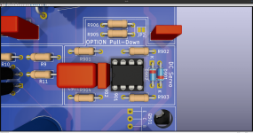
After seeking information about the Output Pull down resistor to the negative rail, suggested in the book to make the OP Amp a Class A Amplifier, I realized that I should add a decoupling capacitor as close as the OP Amp rails.
So I added it, selected in Green on the PCB...


So I added it, selected in Green on the PCB...
What am I missing there?
I read back one of my books, from Self Douglas; "Small Signal Audio Design (English Edition)". I finally found one of his comment on page 160, in the section "The OPA2134 Opamp" that help me choose an appropriate OPAmp for the DCServo.
He wrote (I quoted):
Does anyone have experience with DC servo that he/she could share? Does my schematic is right? I even tried the Pull-down resistor (R905, R906) to the -rail without better result.
I read back one of my books, from Self Douglas; "Small Signal Audio Design (English Edition)". I finally found one of his comment on page 160, in the section "The OPA2134 Opamp" that help me choose an appropriate OPAmp for the DCServo.
He wrote (I quoted):
I found a LTSpice model on one thread here. So I replaced the TL072 with an OPA2134 in both my parts list and my schematic. They are pin compatible! With it, I never got any clipping at 10 Hz. But again, in the simulation, I cannot achieve a DC voltage close to 0 at the output. The closest to the -33.901654mV without DC servo that I can reach with the DC servo is -233.51666mV, and this is with both 1MOhms resistors at the input (R904) and the output (R901) of the DCServo.I have used it many times as a DC servo in power amplifiers, the low bias currents allowing high resistor values and corresponding small capacitors.
Does anyone have experience with DC servo that he/she could share? Does my schematic is right? I even tried the Pull-down resistor (R905, R906) to the -rail without better result.
Attachments
So in my quest to respect the original design of figure 14.17 with it's DC Servo, but still without adequate results in LTSpice, I did some research on the Internet and came across this article which seriously made me doubt the relevance of integrating a DC Servo circuit into my PCB.
As my circuit is already finished, I had two choices:
The former would give me a future development circuit, while allowing me to finish my DIY amplifier with C2, but with an empty PCB section; the DC Servo without its components.
The second choice would result in a completely finished product with very acceptable specifications.
So I first modified the circuit, out of curiosity, to allow easy modification between the two designs with two jumpers; JP1 and JP2. This modification would require soldering to connect the jumpers. JP1 would short-circuit capacitor C2 and bring resistor R4 directly to ground. Adding the OP amp in its socket would finalize the DC Servo circuit. A second JP2 option would connect resistors R905 and R906 to -15 VDC to force the OP amplifier into Class A (Pull-Down OPTION).
Where I have a doubt is the consequence of the JP1 jumper when not soldered. Could it create residual capacitance in the R4/C2 audio path? My idea of creating this jumper rather than simply removing C2 and connecting its pads with a soldered wire was that I could quickly and easily switch from one version to another with a simple solder, rather than constantly removing and replacing C2 in the circuit when testing.
What do you think? Does anyone have an opinion to share?
As my circuit is already finished, I had two choices:
- Preserve the DC Servo section, since it's already drawn, and allow the options of choosing either the DC Servo circuit or the C2 capacitor.
- Remove the entire DC Servo section and preserve the C2 capacitor in the Feedback circuit, in order to obtain a clean final product.
The former would give me a future development circuit, while allowing me to finish my DIY amplifier with C2, but with an empty PCB section; the DC Servo without its components.
The second choice would result in a completely finished product with very acceptable specifications.
So I first modified the circuit, out of curiosity, to allow easy modification between the two designs with two jumpers; JP1 and JP2. This modification would require soldering to connect the jumpers. JP1 would short-circuit capacitor C2 and bring resistor R4 directly to ground. Adding the OP amp in its socket would finalize the DC Servo circuit. A second JP2 option would connect resistors R905 and R906 to -15 VDC to force the OP amplifier into Class A (Pull-Down OPTION).
Where I have a doubt is the consequence of the JP1 jumper when not soldered. Could it create residual capacitance in the R4/C2 audio path? My idea of creating this jumper rather than simply removing C2 and connecting its pads with a soldered wire was that I could quickly and easily switch from one version to another with a simple solder, rather than constantly removing and replacing C2 in the circuit when testing.
What do you think? Does anyone have an opinion to share?
Attachments
-
 09-DC Servo classe A JP2.png413.4 KB · Views: 38
 -
 08-DC Servo classe A JP2.png126.3 KB · Views: 56
 -
 07-DC Servo classe A JP2.png38.4 KB · Views: 55
 -
 06-DC Servo option JP1.png178.8 KB · Views: 50
 -
 05-DC Servo option JP1.png133.6 KB · Views: 46
 -
 04-DC Servo option JP1.png38.5 KB · Views: 44
 -
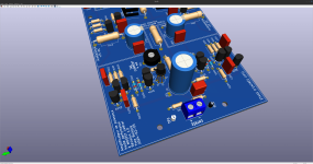
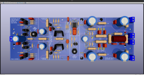 03-Vue de dessus perspective.png388.8 KB · Views: 43
 -
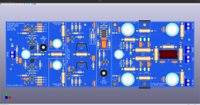 02-Vue de dessus.png190.9 KB · Views: 30
 -
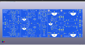 01-Sérigraphie.png139.9 KB · Views: 36
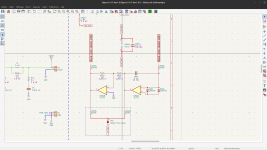
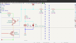
there is an error, your non-inverting input is not grounded, it needs to be tied to gndDoes anyone have experience with DC servo that he/she could share? Does my schematic is right?
look attach
Attachments
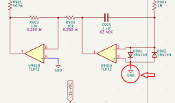
AAAHHHHHHHHHHHHHHHHHHHHHHHHHHHHH!!!!!!!!!there is an error, your non-inverting input is not grounded, it needs to be tied to gnd
look attach
SO MANY THANKS ! ! !!
You are dam right! I missed this tiny little triangle lol...
Now I got 6.6963926uV at the output ... Finally ! ! !
I waited the whole weekend for a comment before proceeding to the PCB fabrication. You have made my day my friend!
Thank you.
Now I am still face with the decision to keep C2 as an option... Hum... What would you do? ;-)
where to put it? I read the topic - I didn’t understand anything, there are a lot of graphs with unstable transient processes, where is C2 and why to set it...Now I am still face with the decision to keep C2 as an option... Hum... What would you do? ;-)
Can I see the diagram in a readable format?
Read post #105. Images attached there. The goal is to have the choice to use either the C2 capacitor or the DC Servo circuit.Can I see the diagram in a readable format?
As for the schematic, please find below both the ASC LTSpice version and the PDF output of my KiCad schematic software.
Attachments
Ok, I read it - everything is clear.Read post #105. Images attached there. The goal is to have the choice to use either the C2 capacitor or the DC Servo circuit.
In your case, you have chosen the wrong connection point for the DC servo.
The more preferable option would be with a capacitor, which it would be desirable to increase to 220 µF.
What do you mean? I choose the same point as of the original design.In your case, you have chosen the wrong connection point for the DC servo.
What do you mean? I choose the same point as of the original design.In your case, you have chosen the wrong connection point for the DC servo.
Just to be clear, this board isn't fabricated yet. It is just on the drawing table by now. There is still time to make any modification before I made it fabricated...
Do you seriously think that they connected the DС servo correctly?What do you mean? I choose the same point as of the original design.
if you look at the DС servo as a first-order filter with a cutoff frequency that penetrates the audio range at a frequency of 20 Hz at a level of -42 dB, with a phase of -90 degrees. Those. this level will be subtracted from the open loop gain. With a gain of 140dB from the DC input, the servo will only retain 100dB and rotate the phase, and so on.
This action of the DС servo can be removed by changing the connection point.
Last edited:
It's my first time with DCServo. I simply copied the original design.Do you seriously think that they connected the DС servo correctly?
What would be your way to connect it?
They installed a DC servo here because of the different resistances R1 and R6+R7, i.e. It is better not to use this amplifier without a DC servo.What do you mean?
If the resistors in the gates of the input stage were equal, the connection point could be formed separately from the alternating signal and the current could be controlled through the emitter resistors of the current mirrors of the diff stages.
As far as I remember, there was no C2 in the original design.I simply copied the original design.
and you shouldn't have it. This capacitor can only appear if the gate resistors are equal, this condition is not met for you, it’s difficult for me to understand what you want to determine by ear?
let it stay that way.n the PCB, the entry point of the DC Servo is connected to the L1 coil and the Output of the DC Servo is connected just before the Feedback R4 Resistor.
I understand very well that this may look confusing. I don't know if you had read the whole thread, and I could easily understand that someone would jump into the latest post. I am doing it myself ;-)As far as I remember, there was no C2 in the original design.
and you shouldn't have it. This capacitor can only appear if the gate resistors are equal, this condition is not met for you, it’s difficult for me to understand what you want to determine by ear?
But for the history, I made a first PCB from a schematic in G. Randy Stone book. It was my mistake to blindly trust the book, I learn it here from all the comments. So I started over with this schematic from Figure 14.17 of Bob Cordell book. And this time I don't want to make a mistake!
Following the schematic, BUT, with my missing ground mistake of your post #106, I never achieve successful result in LTSpice, so I read more on the DC Servo subject.
In the hope to maybe have different results on a real PCB, and in the contrary still have a backup solution, I choose to add the C2 option.
My goal wasn't to have two setups for comparison purpose, but instead have the DC Servo circuit in the hope to make it work, and have the C2 circuit in case I couldn't make it work with the DC Servo.
Now in conclusion, with your good eyes having found my mistake, the C2 isn't necessary anymore. So yesterday I remake my schematic and PCB drawings to reflect the DC Servo circuit, removing entirely the C2 capacitor.
For the interest, I attached the new clean version of the PDF and LTSpice version below. Be aware that I renamed some resistors and capacitors.
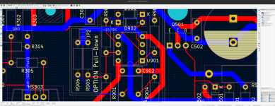
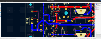
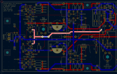
As for the DC Servo Input/Output, I make it sure that the traces were reflecting the schematic. The Input of the DC Servo is taken directly from the R12 pad, and it's trace is in a unique path highlighted here:
As well as it's output that goes with a single trace to the pad of R5, again highlighted here:
So I would say that I am ready to proceed with the fabrication of this new PCB, unless an experimented user have real concerns about this configuration. And I am very open to hear it because as mentioned above, I don't want to miss it this time ;-)
In another subject, you may notice that in the schematic, the gate resistors of the Lateral MOSFETs are only 100 Ohms. I remember having read in the past that it is not suggested to go below 220 Ohms for those. But with the originals 470 Ohms, I observed ringing at 20 kHz, both in the Square Waves and Sinusoidal Waves simulations.
So I made simulations with their values at 680 Ohms, 470 Ohms, 330 Ohms, 220 Ohms. I achieved no ringing only with 100 Ohms. I decided then to compare the THD of each values and surprisingly, I got the best THD and the best Slew Rate with 100 Ohms.
So what exactly is the risk to go as low as 100 Ohms? Oscillations? I got them with the higher values !...
Attachments

With the use of C2, you initially made the wrong conclusions; the condition for its appearance is the equality of the gates resistors in the input stages Jfets at nominal value. Because if this is not the case then C2 should not appear in the diagram.In the hope to maybe have different results on a real PCB, and in the contrary still have a backup solution, I choose to add the C2 option.
My goal wasn't to have two setups for comparison purpose, but instead have the DC Servo circuit in the hope to make it work, and have the C2 circuit in case I couldn't make it work with the DC Servo.
I don’t know who recommended that you not make the value of this resistor less than 220 ohms, a logical explanation for this is needed.In another subject, you may notice that in the schematic, the gate resistors of the Lateral MOSFETs are only 100 Ohms. I remember having read in the past that it is not suggested to go below 220 Ohms for those. But with the originals 470 Ohms, I observed ringing at 20 kHz, both in the Square Waves and Sinusoidal Waves simulations.
The value of this resistor must be selected to the minimum, so that it blocks the parasitic capacitances of the drain and source junctions through the gate, so that the transistor cannot turn on spontaneously at high frequencies, i.e. "ring".
In your case, in the model this value was 100 ohms, so use it.
Thank you very much for all your comments and help Hennady! I appreciated itIn your case, in the model this value was 100 ohms, so use it.
")
- Home
- Amplifiers
- Solid State
- A Lateral MOSFET Power Amplifier Design (second try)