Got it...!It looks like you took the feedback source from the wrong location. It should come directly from the output inductor, not the opposite end of the output rail.
It is all about the load impedance.
For 4 ohms it is better to use two pairs of outputs.
For 2 ohms even more.
Just make sure your drivers are able to actually drive those that is all.
Adding more transistors at the output stage splits the current between them allowing for less heat and more optimized safe operating area - that is graph you can find in the datasheet for each particular MOSFET.
Last edited:
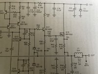
This is one view I don't get right. Where is the source of the +Vrail? From the right of R46 or from the left of C10?? You say to isolate the MOSFETs from the rail with a 10 Ohms resistor. In this schematic, if the source of the +Vrail is on the right of R46, the R10 don't isolate the MOSFET!R45 isolation resistor.
My understanding of the layout of this schematic is that the +Vrail is coming from the right of R46, goes to the MOSFETs, and pass into R10 to continue to the VAS and IPS stage. Am I right?
Here is another question I asked before without any answer. Let's say I revert my design back with two pairs of MOSFETs (references aren't updated yet in my screenshot s below). Referring to the original Figure 14.17 of the book, there is a note saying "+55V @ load" between R45 and R46. So I do expect that on the left of R10 we would get a bit less than +55V.
Seeing that the rail voltage seem to go to the VAS/IPS section on the left of C10, I would draw my schematic like this:

But referring back to the Figure 9.20 Example IPS-VAS, the +Vrail are still at +55V. That make me thing I should draw my schematic like this:

Does everyone see the difference where my R506 is taped?
Which connection is right for the +Vrail of the VAS-IPS? Before R506 or after R506? Those C502/C503 would only filter the Drivers in one case, while they would also filter the VAS-IPS in the other case...
Seeing that the rail voltage seem to go to the VAS/IPS section on the left of C10, I would draw my schematic like this:
But referring back to the Figure 9.20 Example IPS-VAS, the +Vrail are still at +55V. That make me thing I should draw my schematic like this:
Does everyone see the difference where my R506 is taped?
Which connection is right for the +Vrail of the VAS-IPS? Before R506 or after R506? Those C502/C503 would only filter the Drivers in one case, while they would also filter the VAS-IPS in the other case...
Which connection is right for the +Vrail of the VAS-IPS? Before R506 or after R506? Those C502/C503 would only filter the Drivers in one case, while they would also filter the VAS-IPS in the other case...
After R506. You want to “isolate “ VAS and IPS from large currents in the OPS.
You will need to use same drivers and output transistors as is drawn in the book.I guess what I am looking for is one circuit, based on MOSFETs, that is already very well designed so I can simply reproduce it.
If you change either one or both you will need to make adjustments to schematics and tap into engineering as a result. Which simply means lots and lots of simulations. This is the way.

Here is safe operation area graph for MOSFET you are using. At 50V you are looking at 2.5A DC current.
If you want 70W power that is approximately 16Vrms to the load. If the load is 4 ohms you need to supply 10/4 = 4Amps to the load.
I’d use a pair of outputs.

If you want 70W power that is approximately 16Vrms to the load. If the load is 4 ohms you need to supply 10/4 = 4Amps to the load.
I’d use a pair of outputs.
I would use 1 pair of double-die mosfets ECW20N20 / ECW20P20.
This way they come pre-matched from the factory, no need to match them by the builder.
If using 2 pairs (single die) they will need to be matched for Vgs. Otherwise amp WILL oscillate.
This way they come pre-matched from the factory, no need to match them by the builder.
If using 2 pairs (single die) they will need to be matched for Vgs. Otherwise amp WILL oscillate.
So... Like this..., right?After R506. You want to “isolate “ VAS and IPS from large currents in the OPS.
Why? I already have 8 x 0,1uF Polypropylene Film capacitor, WIMA MKS 2... The 1uF are 7,2 x 7.2mm. The 0,1uF are only 7.2 x 2.5 mm!C18,C19 bypass caps. Can safely increase those to 1uF and use film type.
And we're back lolol... I already have ECX10x20, I don't want to buy other parts seeing their price. Not to mention the JFET of the IPS $$$I would use 1 pair of double-die mosfets ECW20N20 / ECW20P20. This way they come pre-matched from the factory, no need to match them by the builder.
I don't want either to buy new ECX10x20 to mach them.If using 2 pairs (single die) they will need to be matched for Vgs. Otherwise amp WILL oscillate.
So I guess I'm stuck! Unless I design for 1 pair only with less power output.
Just for my understanding. I looked at the datasheet of the EXW20x20. Beside their TO264 package, I don't see any other physical difference. What does mean exactly double-die? Is it that their are two MOSFET into one casing?
These Exicons, even 1 pair, are very robust. I'm sure they will be fine at 4 Ohms, unless you are planning to play square waves instead of music...
Yes. Their.
Is it that their are two MOSFET into one casing?
Yes. Their.
One argument in my favor is that I am leaving in a condominium. My actual system include one Power Amplifier Rotel RB-1552 MKII (130 WRMS) that I can't raise that much if I don't want my neighbor coming knock on my door!These Exicons, even 1 pair, are very robust. I'm sure they will be fine at 4 Ohms, unless you are planning to play square waves instead of music...
Still, I maybe could plan for TO264 physical package for future...
Thanks!!!Spice models available from the Toshiba website if I remember correctly
Here what I used:
I have a design question...
In my version of the asc file above, The protections diodes D502/D602 have their cathode and anode respectively connected to the Feedback path from the L1 output inductance and to the Sources of both MOSFETs. I understand that they aren't active unless the protection came up, but what is the physical best path for their traces? Is it ok to connect them directly to the Sources traces or they should be connect instead to the L1 pad? Considering that both the Sources pins and the L1 pin are away physically one from the others. Based on the preceding remarks, I am keeping the Sources traces away from the Feedback traces as much as I can.
In my version of the asc file above, The protections diodes D502/D602 have their cathode and anode respectively connected to the Feedback path from the L1 output inductance and to the Sources of both MOSFETs. I understand that they aren't active unless the protection came up, but what is the physical best path for their traces? Is it ok to connect them directly to the Sources traces or they should be connect instead to the L1 pad? Considering that both the Sources pins and the L1 pin are away physically one from the others. Based on the preceding remarks, I am keeping the Sources traces away from the Feedback traces as much as I can.
Am I using LTSpice the right way?
I was studying the LTSpice chapter while comparing in parallel both the book example design results and the Figure 14.17 design ones, the later modified with my drivers and MOSFETs Output parts.
At the Square-Wave Response section, I was unable to reach a top square wave without ringings unless I increased the C301/401 Millers capacitors of 10pF from the original design to 35pF in my design. But once I achieved that, I had doubts about a possible difference between the original parts and my parts choice.
I compared the MOSFETs data-sheets versus the original one and my MOSFETs was exceeding the original specifications. So I started a new set of tests, this time comparing the original parts of Figure 14.17 with my parts design of the same Figure 14.17, with the same 10pF values for both Miller capacitors. And in order to keep the original parts design accurate, I copied/pasted the model parts from Bob Cordell library text file into my MyParts.lib file. You will find both asc files and my library attached. You may have to rename it and modify the .lib path of the schematic!
After having calibrated each design RVx variable resistors to reach the same DC Analysis, I proceed to the Frequency Response tests, I had two peak from each design. But the peak of the original design was only a 123.20933mdB at about 500KHz while my design had 4.5633216dB at about 851KHz ! The original design is always the top one in all screen shots...

Then I started to raise the C301/401 Miller capacitors from 10pF until I had an acceptable peak in the order of the original design. I reach a maximum peak of 9.609829mdB around 122KHz with 35pF, the same value of my preceding Square Waves tests!

Then I compared the cutoff frequency of -3dB for both designs. The original design have a cutoff frequency of 1.76MHz at -3dB while mine have only 556KHz at -3dB. Would you consider this acceptable for a design?

I was studying the LTSpice chapter while comparing in parallel both the book example design results and the Figure 14.17 design ones, the later modified with my drivers and MOSFETs Output parts.
At the Square-Wave Response section, I was unable to reach a top square wave without ringings unless I increased the C301/401 Millers capacitors of 10pF from the original design to 35pF in my design. But once I achieved that, I had doubts about a possible difference between the original parts and my parts choice.
I compared the MOSFETs data-sheets versus the original one and my MOSFETs was exceeding the original specifications. So I started a new set of tests, this time comparing the original parts of Figure 14.17 with my parts design of the same Figure 14.17, with the same 10pF values for both Miller capacitors. And in order to keep the original parts design accurate, I copied/pasted the model parts from Bob Cordell library text file into my MyParts.lib file. You will find both asc files and my library attached. You may have to rename it and modify the .lib path of the schematic!
After having calibrated each design RVx variable resistors to reach the same DC Analysis, I proceed to the Frequency Response tests, I had two peak from each design. But the peak of the original design was only a 123.20933mdB at about 500KHz while my design had 4.5633216dB at about 851KHz ! The original design is always the top one in all screen shots...
Then I started to raise the C301/401 Miller capacitors from 10pF until I had an acceptable peak in the order of the original design. I reach a maximum peak of 9.609829mdB around 122KHz with 35pF, the same value of my preceding Square Waves tests!
Then I compared the cutoff frequency of -3dB for both designs. The original design have a cutoff frequency of 1.76MHz at -3dB while mine have only 556KHz at -3dB. Would you consider this acceptable for a design?
Attachments
Just a heads up, Digikey seems to start stocking esotering jfets again.
https://www.digikey.nl/en/products/detail/linear-integrated-systems-inc/lsk489-soic-8l-rohs/16649372
https://www.digikey.nl/en/products/detail/linear-integrated-systems-inc/lsk489-soic-8l-rohs/16649372
I've made a lot of progress since my last post.
I finished reading my book "Designing Audio Power Amplifiers" by Bob Cordell.
I revised the schematic in figure 14.17
I ran a ton of simulations, comparing the design with the original transistors in the figure versus my transistors so I could get my inventory parts back.
I finally identified the cause of the differences in distortion between the transistor choices. With the TTC004B and TTA004B transistors replacing the 2SC3503C and 2SA1381C respectively, I get virtually the same harmonic distortion results.
However, with the replacement of the MOSFET transistors 2SK134C and 2SJ149C by 10N20 and 10P20 respectively, the harmonic distortion increases.

I've finished drawing the PCB and am ready to have it manufactured. But first, I follow Bob Cordell's advice to simulate the DCServo circuit properly. Now I've got a problem!
Decoupling the output of the DCServo circuit, I measure a DC voltage of -33.9614mV. When I connect its output to the Feedback input, this voltage rises to -1.4919597V!
No matter how I play with the values of the 1Meg and 100k resistors, I can't manage to reduce this voltage to a value lower than that obtained without the DCServo. I use a JFET LS072 OP amplifier. I found the LTSpice model on the Internet.
I'm attaching my ASC schematic as well as my library of models for you to play with as needed.
For fun, I'm also attaching a few pictures of what the new PCB will look like.
As for jwihelm comment below:
I tried to route the voltage rails one over the other on their respective side of the board. I admit I don't like how this force a non symmetric design. Plus, it is almost impossible to achieve that from the connectors to the first resistors in series that isolate the +/-55VDC after the MOSFET. The electrolytic cans are so big that the traces never can be one over the other, unless you make them longer. As for the traces after the isolating resistors, I achieved it but didn't like the looks it create. So I looked at two different designs. One from the figure 6.24 from G. Randy Slone book "The Audiophile's Projet Sourcebook", and the other from my reVox B750 Amplifier board (picture attached). Both didn't route their rails voltage one over the other. So with all the decoupling capacitors along their path, I am confident that the noise would be minimize.
Here is the reVox B750 PCB with the +/- rails traces highlighted as well as the ground traces. Notice how the Big cans are physically above the diodes bridge, while the Output collector transistors are feed below this diodes bridge!

And here are my latest PCB version pictures:


Ground traces. All the rails traces, Input traces and Output traces are going individually to the HQG.

Power Rails:

Negative Feedback traces, also isolated from the High current MOSFET return traces.

I finished reading my book "Designing Audio Power Amplifiers" by Bob Cordell.
I revised the schematic in figure 14.17
I ran a ton of simulations, comparing the design with the original transistors in the figure versus my transistors so I could get my inventory parts back.
I finally identified the cause of the differences in distortion between the transistor choices. With the TTC004B and TTA004B transistors replacing the 2SC3503C and 2SA1381C respectively, I get virtually the same harmonic distortion results.
However, with the replacement of the MOSFET transistors 2SK134C and 2SJ149C by 10N20 and 10P20 respectively, the harmonic distortion increases.
I've finished drawing the PCB and am ready to have it manufactured. But first, I follow Bob Cordell's advice to simulate the DCServo circuit properly. Now I've got a problem!
Decoupling the output of the DCServo circuit, I measure a DC voltage of -33.9614mV. When I connect its output to the Feedback input, this voltage rises to -1.4919597V!
No matter how I play with the values of the 1Meg and 100k resistors, I can't manage to reduce this voltage to a value lower than that obtained without the DCServo. I use a JFET LS072 OP amplifier. I found the LTSpice model on the Internet.
I'm attaching my ASC schematic as well as my library of models for you to play with as needed.
For fun, I'm also attaching a few pictures of what the new PCB will look like.
As for jwihelm comment below:
Your next learning curve should be about loop areas in your layout design. + and - rails should be on top of each other so they cancel their noise. Sources should follow returns very closely. Input ground should route very closely to the feedback trace. Otherwise the traces will emit a lot of RF for the sensitive input stage to pick up. As Brian92fs suggests, ground planes are a bad idea. Better to use properly routed traces. Planes are better for high speed (digital) circuits. A single output pair amp should be tiny to minimize loop area.
I tried to route the voltage rails one over the other on their respective side of the board. I admit I don't like how this force a non symmetric design. Plus, it is almost impossible to achieve that from the connectors to the first resistors in series that isolate the +/-55VDC after the MOSFET. The electrolytic cans are so big that the traces never can be one over the other, unless you make them longer. As for the traces after the isolating resistors, I achieved it but didn't like the looks it create. So I looked at two different designs. One from the figure 6.24 from G. Randy Slone book "The Audiophile's Projet Sourcebook", and the other from my reVox B750 Amplifier board (picture attached). Both didn't route their rails voltage one over the other. So with all the decoupling capacitors along their path, I am confident that the noise would be minimize.
Here is the reVox B750 PCB with the +/- rails traces highlighted as well as the ground traces. Notice how the Big cans are physically above the diodes bridge, while the Output collector transistors are feed below this diodes bridge!
And here are my latest PCB version pictures:
Ground traces. All the rails traces, Input traces and Output traces are going individually to the HQG.
Power Rails:
Negative Feedback traces, also isolated from the High current MOSFET return traces.
Attachments
Respect! --does it make more sense to but also the bias spreader on the heatsink....?? with another type of bjt´s of course
- Home
- Amplifiers
- Solid State
- A Lateral MOSFET Power Amplifier Design (second try)