is it something I must also be careful also if I don't the paralleling?
No. You need to match upper pair (N device to N), and lower pair (P device to P).
No need to match upper N device to lower P device.
If using only one pair of devices, there is no need for source resistors.
Great! Right now I am studding the chapter 23 SPICE Simulation from the book. I did the Transient simulation below:No need to match upper N device to lower P device.
If using only one pair of devices, there is no need for source resistors.
But I am a bit curious about the result. Isn't is a bad result with these oscillations on top of the Rising edge? The blue line is the output. the red line is across C2 and the green line is the input.
Good morning,
I revised all the parts in the schematic. I included my own parts library using Bob Cordell parts definitions from his site text file, of course keeping all the copyright related to them. I simply copied/pasted the parts I needed.
I replaced all:
I will still have to check the 10N20 and 10P20 with the data sheets.
Then I have done all the suggested tests of chapter 23 until the 20kHz distortion test. I get these results:
1kHz
20kHz
There is one thing though that I don't understand. the current plot of C401 (lower section) have some spikes.
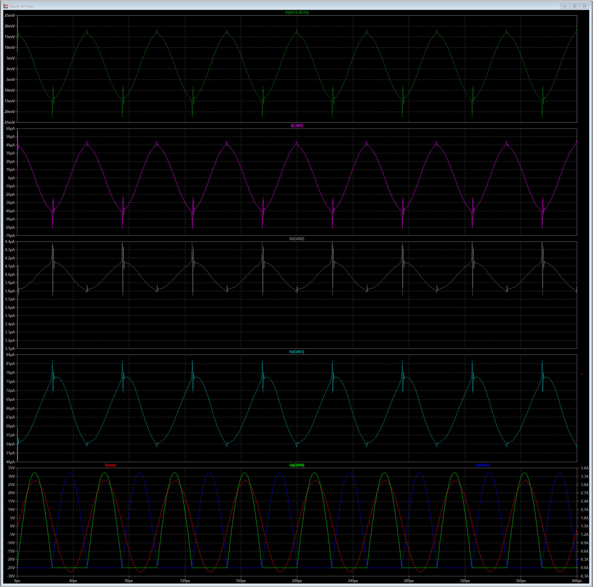
I achieve to remove them if I increase C301/C401 from 10pF to 100pF.
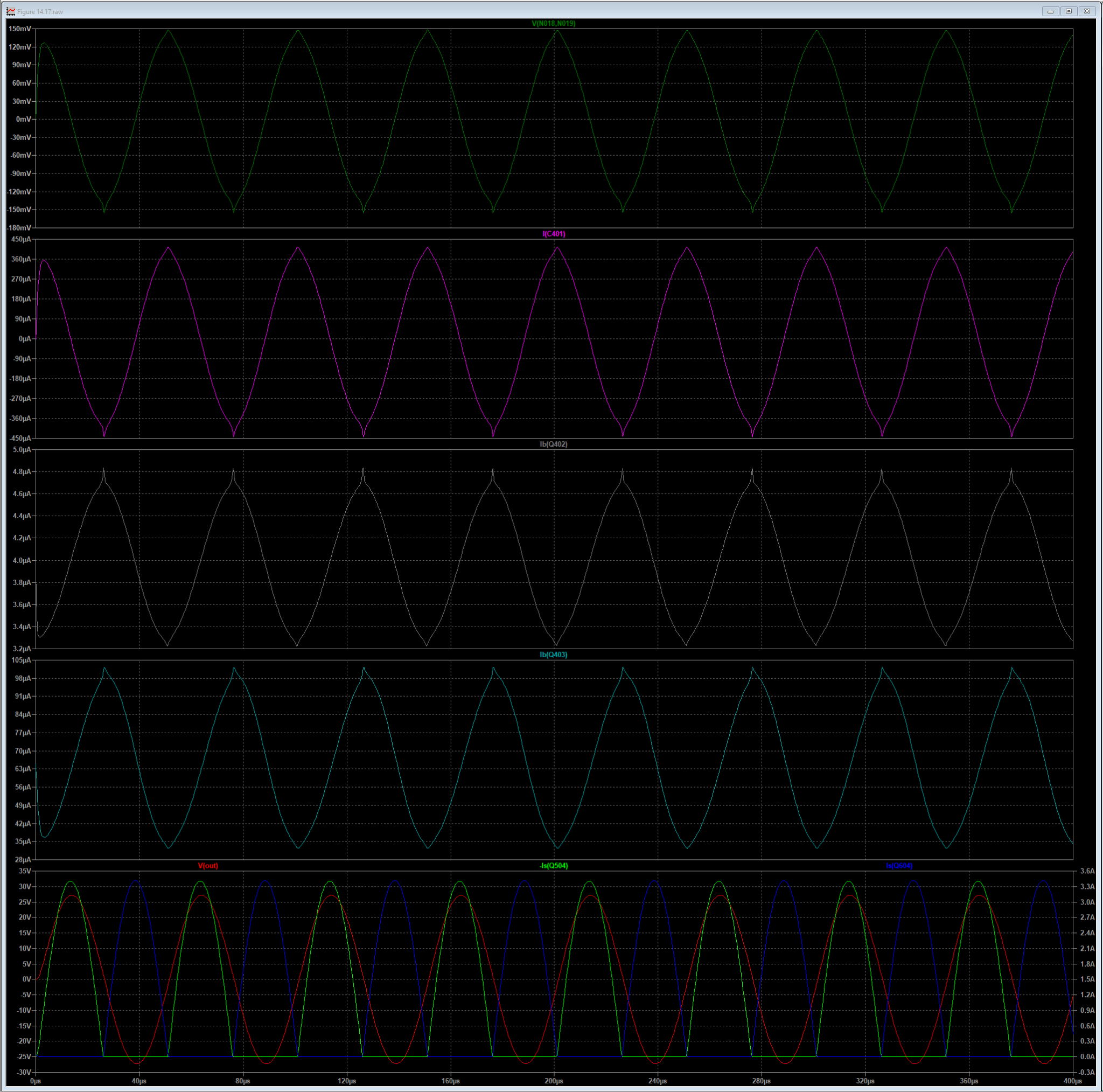
But the distortion at 20 kHz raise to these results:
Is there another part I should modified in order to remove these spikse without altering the THD?
The asc and lib files attached. You will have to rename the extension of the library as .lib The forum doesn't let me attach the original extension.
I revised all the parts in the schematic. I included my own parts library using Bob Cordell parts definitions from his site text file, of course keeping all the copyright related to them. I simply copied/pasted the parts I needed.
I replaced all:
2N5401 with 2N5401C (Bob Cordell)
2N5551 with 2N5551C (Bob Cordell)
KSA1381 with 2SA1581C (Bob Cordell)
KSC3503 with 2SC3503C (Bob Cordell)
1N4148 with 1N4149YB, from Bob Cordell 1N4148C definition, replacing the Iave=200m with Iave=500m for the 1N4149YB.
I will still have to check the 10N20 and 10P20 with the data sheets.
Then I have done all the suggested tests of chapter 23 until the 20kHz distortion test. I get these results:
1kHz
N-Period=8
Fourier components of V(out)
DC component:-0.0327884
Harmonic Frequency Fourier Normalized Phase Normalized
Number [Hz] Component Component [degree] Phase [deg]
1 1.000e+3 2.764e+0 1.000e+0 90.20° 0.00°
2 2.000e+3 2.785e-5 1.008e-5 100.73° 10.53°
3 3.000e+3 6.603e-5 2.389e-5 -170.00° -260.20°
4 4.000e+3 1.506e-5 5.449e-6 96.12° 5.92°
5 5.000e+3 2.070e-5 7.490e-6 -173.91° -264.11°
6 6.000e+3 1.030e-5 3.726e-6 93.64° 3.44°
7 7.000e+3 5.223e-6 1.890e-6 -175.54° -265.74°
8 8.000e+3 6.685e-6 2.419e-6 92.51° 2.31°
9 9.000e+3 1.909e-7 6.906e-8 -0.28° -90.48°
10 1.000e+4 3.911e-6 1.415e-6 91.91° 1.71°
Partial Harmonic Distortion: 0.002799%
Total Harmonic Distortion: 0.002803%
20kHz
Harmonic Frequency Fourier Normalized Phase Normalized
Number [Hz] Component Component [degree] Phase [deg]
1 2.000e+4 2.742e+1 1.000e+0 93.82° 0.00°
2 4.000e+4 4.080e-3 1.488e-4 75.71° -18.11°
3 6.000e+4 9.450e-3 3.446e-4 -177.76° -271.58°
4 8.000e+4 1.686e-3 6.148e-5 58.27° -35.55°
5 1.000e+5 6.795e-3 2.478e-4 176.16° 82.34°
6 1.200e+5 1.370e-3 4.997e-5 38.85° -54.97°
7 1.400e+5 5.270e-3 1.922e-4 172.31° 78.50°
8 1.600e+5 1.332e-3 4.857e-5 23.16° -70.66°
9 1.800e+5 4.419e-3 1.611e-4 168.36° 74.55°
10 2.000e+5 1.430e-3 5.213e-5 13.13° -80.69°
Partial Harmonic Distortion: 0.052583%
Total Harmonic Distortion: 0.096613%
There is one thing though that I don't understand. the current plot of C401 (lower section) have some spikes.
I achieve to remove them if I increase C301/C401 from 10pF to 100pF.
But the distortion at 20 kHz raise to these results:
N-Period=4
Fourier components of V(out)
DC component:-0.0343079
Harmonic Frequency Fourier Normalized Phase Normalized
Number [Hz] Component Component [degree] Phase [deg]
1 2.000e+4 2.721e+1 1.000e+0 100.83° 0.00°
2 4.000e+4 3.365e-2 1.237e-3 104.95° 4.12°
3 6.000e+4 8.491e-2 3.121e-3 -136.06° -236.89°
4 8.000e+4 1.386e-2 5.093e-4 112.90° 12.07°
5 1.000e+5 5.254e-2 1.931e-3 -115.24° -216.07°
6 1.200e+5 1.043e-2 3.833e-4 120.26° 19.43°
7 1.400e+5 3.583e-2 1.317e-3 -93.92° -194.75°
8 1.600e+5 8.896e-3 3.270e-4 131.72° 30.89°
9 1.800e+5 2.615e-2 9.612e-4 -74.70° -175.53°
10 2.000e+5 8.065e-3 2.964e-4 145.74° 44.91°
Partial Harmonic Distortion: 0.427295%
Total Harmonic Distortion: 0.452002%
Is there another part I should modified in order to remove these spikse without altering the THD?
The asc and lib files attached. You will have to rename the extension of the library as .lib The forum doesn't let me attach the original extension.
Attachments
BZX384B10 models can't be found in ltspice. better replace it, like I did before, with any other 10V zener, that belongs to lt spice...
Those spikes are the feedback reacting to the cross-over by jumping into action. Suppress the spikes and the feedback is doing less correction, hence distortion rises. Reducing those spikes and the distortion probably requires careful attention to the bias-point and switch-off sequence of the outputs and drivers. Lots of people have played with designs that never fully turn-off the drivers and outputs to reduce the transients like this.
Ugly spikes on current (collectors of VAS devices Q303/Q403).
Increase OS idle current (currently 24mA) to get rid of them. I just tried 270mA (Rv2 set to 222), and spikes are almost gone (acceptable at 20kHz).
270mA is of courser too much, but it shows that increasing it will improve the problem. 24mA seems too low....
You may also need to experiment with VAS current - it's only 6mA, kind of lowish....
Last edited:
@minek123 Which one do you use? I find them in the LTSpice standard.dio libraryBZX384B10 models can't be found in ltspice. better replace it, like I did before, with any other 10V zener, that belongs to lt spice...
yvesboisjoly@Defiant:/mnt/Windows11/Users/yvesb/AppData/Local/LTspice/lib/cmp$ grep -i BZX384B10 *
standard.dio:.model BZX384B10 D(Is=1.13E-14 N=1.103 BV=10 IBV=0.005 Rs=0.4798 Cjo=6.004E-11 Vj=0.6305 M=0.3302 Fc=0.5 Iave=250M Vpk=10 Mfg=NXP Type=ZENER)
Just select any 10V Zener from the list.... E.g. KDZ10B
My ltspice definitely doesn't know BZX384B10...
My ltspice definitely doesn't know BZX384B10...
Also, if you are doing 'real' simulation, it's time to replace voltages V4/V5 with real stuff (Zeners, CCS, etc...).
I achieve to remove them if I increase C301/C401 from 10pF to 100pF
That may work, but it will make your amp much slower. You want it fast, and without spikes 🙂
You need to find an optimum between compensation and currents in VAS and OS.
And then you need to sim it with squares, and then look at FFT plot.
And then make is stable (Phase margin and gain margin).
Good project for long winter evenings 🙂
You mean KDZV10B ? It's the only one close I get from the listJust select any 10V Zener from the list.... E.g. KDZ10B
Well they are gone with the new zener above!Ugly spikes on current (collectors of VAS devices Q303/Q403).
Increase OS idle current (currently 24mA) to get rid of them. I just tried 270mA (Rv2 set to 222), and spikes are almost gone (acceptable at 20kHz).
270mA is of courser too much, but it shows that increasing it will improve the problem. 24mA seems too low....
I used RV2=260 Ohms and got:
Id(Q604): -0.20796 device_current
Thanks! I was actually looking what could modify to get it at 200mA. (I am learning here ;-) )
Actually, I am not yet ready to design the Power Supply. In the real world, I am using my two Rigol DP712 Programmable Power Supply (55 VDC/3A).Also, if you are doing 'real' simulation, it's time to replace voltages V4/V5 with real stuff (Zeners, CCS, etc...).
Once two boards (stereo )will be finished and working, I will proceed with the Power Supply.
Yes you said it! And I am kind of impatient to use my new scope lol!Good project for long winter evenings 🙂
And that will be modifying R?? 🙂You may also need to experiment with VAS current - it's only 6mA, kind of lowish....
This design is very different from the preceding one I tried. And the fact that it is spread on two Figures in the book doesn't help to find were is the frontier between each stages... I mean, the group R501/R502/RV2/Q501/Q502 are part of the VAS or the OPS? What about D501/D502/D601/D602/R504/R605?
If the OPS start at the driver Q503/Q603, then all those above are under the VAS stage, and if yes, I should rename all them from 5xx/6xx to 3xx/4xx for my own comprehension. I like to have each stage starting at a series number.
Actually, I am not yet ready to design the Power Supply. In the real world, I am using my two Rigol DP712 Programmable Power Supply (55 VDC/3A).
I'm not talking about main power supply. In input stage I see two ideal voltage sources, V4 and V5.
These are ideal voltage sources (a 'shortcuts' provided by ltspice), that in your real amp will be replaced by 'real' circuitry.
E.g. +15V voltage source can be done with R+ Zener from the positive rail, and -15V R + Zener from negative rail.
Or from separate, small, regulated PSU.
> You may also need to experiment with VAS current - it's only 6mA, kind of lowish....
And that will be modifying R??
Your VAS devices are Q303/Q403, their current is controlled by resistors in their emitters: R303/R403
R501/R502/RV2/Q501/Q502 are part of the VAS or the OPS?
This is bias spreader (also called Vbe multiplier). Check the book, it has a chapter on it.
It controls the idle current of the OPS, based on thermal feedback from the OS devices.
It's sandwiched between VAS and OS.
D501/D502/D601/D602/R504/R605
OS protection circuit. Also should be described in the book somewhere.
Yes got it! Those come from my KiCad schematic, where I had already put the necessary parts.I'm not talking about main power supply. In input stage I see two ideal voltage sources, V4 and V5.
But seeing that KiCad wasn't good at all for simulation I started replacing them in KiCad and that modification has follow into this LTSpice schematic... I'll take care of them...
Ah great. I already start playing with them, So I do understand stuff lol ;-)Your VAS devices are Q303/Q403, their current is controlled by resistors in their emitters: R303/R403
Thanks! Now I remember having saw them in the movie of Bob Cordell. I also remember having read the chapter in the book but I probably have to much in my head since the beginning of this project to untangle it all from the preceding one.This is bias spreader (also called Vbe multiplier). Check the book, it has a chapter on it.
It controls the idle current of the OPS, based on thermal feedback from the OS devices.
It's sandwiched between VAS and OS.
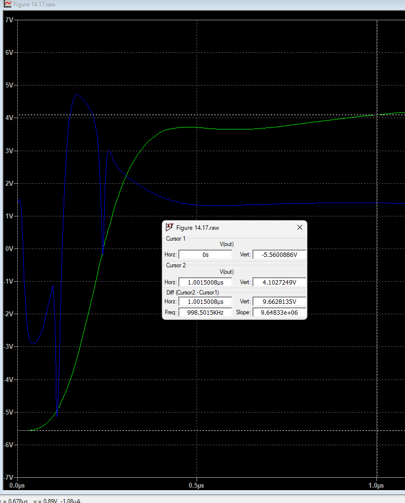
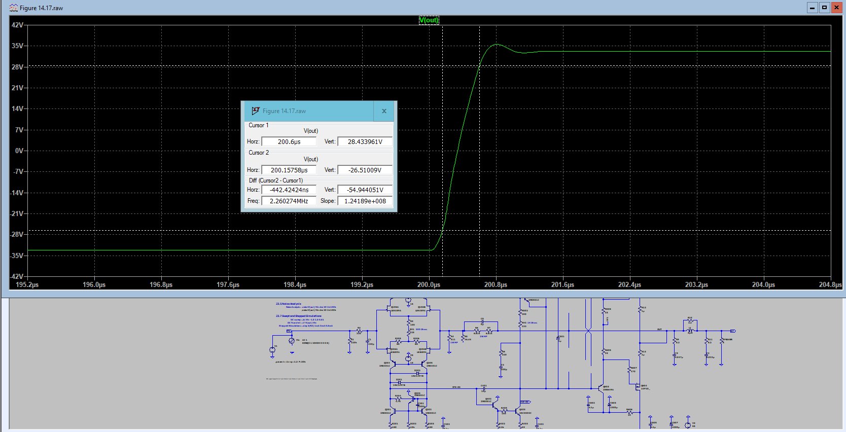
I did the Square-Wave Response test at 50kHz from page 561. The book says "Read the indicated slew-rate in the bottom right portion of the information box"
In my software version, I don't see that slew-rate fields. Is is the result of the "Vert/Horz" field? In my case it would be:
Vert: 9.6628135V
Horz: 1.0015008us
In my software version, I don't see that slew-rate fields. Is is the result of the "Vert/Horz" field? In my case it would be:
Vert: 9.6628135V
Horz: 1.0015008us
9V/us ??
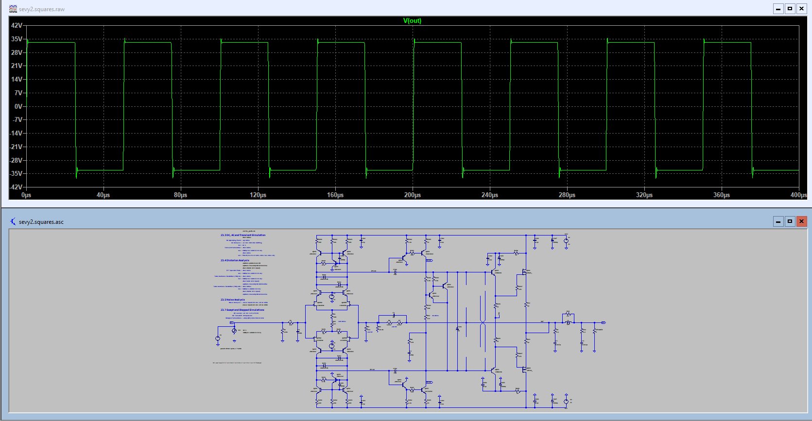
Here is my quick sim of square waves:
Slew rate approx 120 V/us.
These squares need to be fixed, as there is an overshot. Check at 1kHz first.
I removed some stuff (unimportant for the actual sim) from the schematic (protection circuits; usually I add them at the end) to avoid clutter.
Slew rate approx 120 V/us.
These squares need to be fixed, as there is an overshot. Check at 1kHz first.
I removed some stuff (unimportant for the actual sim) from the schematic (protection circuits; usually I add them at the end) to avoid clutter.
Attachments
Please note - the faster the amp (slew rate), the more difficult to make it stable in the actual build.
For a 100W amp, 20V/us is sufficient.
For a 100W amp, 20V/us is sufficient.
I don't get it...
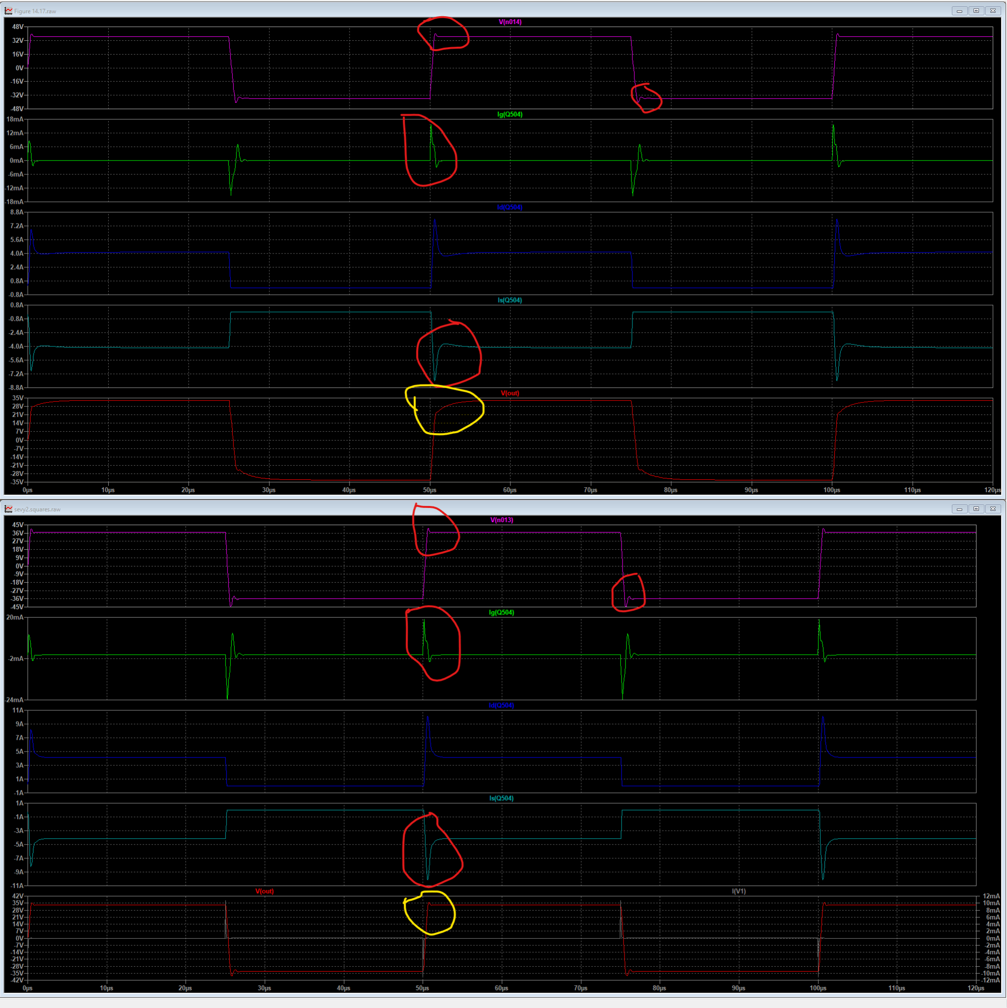
I putted your drawing and mine side by side and checked everything. I added your parameters of the Vin and the two resistor 1uOhm at the source of each MOSFET.
When I compare the signals, I have exactly the same square pulse on both simulation until I reach the MOSFETs. The signal are the same before R507. They are very close at the gate of each MOSFET. But at the drain and the source, they differ.
Both MOSFETs model come from the same library. But it look's like they doesn't give the same result.
In the capture below, the upper traces come from my asc and the lower traces come from your asc.
Attach you asc file.
I added them so I can easily see what is the OS current. They don't have any other function.
What is idle OS current in your sim? In mine Rv2 is set to 222 Ohm. Idle current is 270mA, most likely that's why my squares look different.
resistor 1uOhm at the source of each MOSFET.
I added them so I can easily see what is the OS current. They don't have any other function.
What is idle OS current in your sim? In mine Rv2 is set to 222 Ohm. Idle current is 270mA, most likely that's why my squares look different.
- Home
- Amplifiers
- Solid State
- A Lateral MOSFET Power Amplifier Design (second try)