Changes for BF245B
Sir, What are the canges to be made for BF245B?
Thanks and regards,
Sumesh
VR 1k must be replaced with 4k7 for BF245A, and regulation output voltage will be from +/12V to +/-24V.
Sir, What are the canges to be made for BF245B?
Thanks and regards,
Sumesh
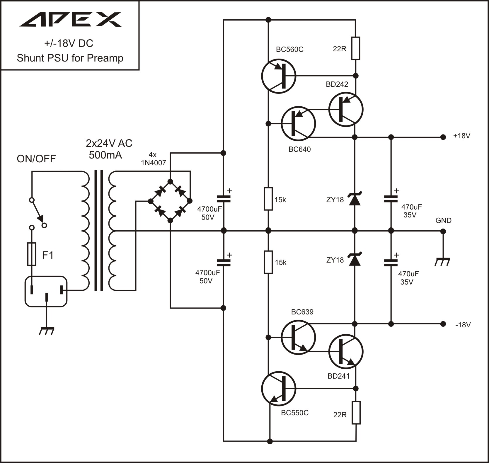
Gentlemen, please note a drawing error in the preamp schematic of post 4
http://www.diyaudio.com/forums/power-supplies/164365-class-preamp-psu.html#post2141076.
Polarity of all four output transistors is wrong, or in other words you have to
use p-channel, n-channel, n-ch., p-ch. reading from top of the picture to bottom.
I also doubt that 2N3268 and 2N3269 are designations of Junction Fets.
As far as I can see these observations have not been reported here before.
Nevertheless the circuit should work considering these points. Searching for
these transistors leads to another DIYA page 100W Ultimate Fidelity Amplifier
where the point was already addressed: "Fets are K170 and J74" and Apex
corrected the scheme in post 56 over there
100W Ultimate Fidelity Amplifier
However the intention of this thread was to promote the shunt regulator of post 1
http://www.diyaudio.com/forums/power-supplies/164365-class-preamp-psu.html#post2140391
and it certainly deserves more attention.
Hi,
I am looking at the A class PSU only, not on the preamp...
Thanks
I am looking at the A class PSU only, not on the preamp...
Thanks
Gentlemen, please note a drawing error in the preamp schematic of post 4
http://www.diyaudio.com/forums/power-supplies/164365-class-preamp-psu.html#post2141076.
Polarity of all four output transistors is wrong, or in other words you have to
use p-channel, n-channel, n-ch., p-ch. reading from top of the picture to bottom.
I also doubt that 2N3268 and 2N3269 are designations of Junction Fets.
As far as I can see these observations have not been reported here before.
Nevertheless the circuit should work considering these points. Searching for
these transistors leads to another DIYA page 100W Ultimate Fidelity Amplifier
where the point was already addressed: "Fets are K170 and J74" and Apex
corrected the scheme in post 56 over there
100W Ultimate Fidelity Amplifier
However the intention of this thread was to promote the shunt regulator of post 1
http://www.diyaudio.com/forums/power-supplies/164365-class-preamp-psu.html#post2140391
and it certainly deserves more attention.
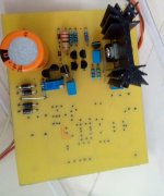
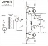
This PSU I use for SS Preamp. Output voltage +/-24Vmax.
Attachments
Hi,
I am looking at the A class PSU only, not on the preamp...
Thanks
And I was reporting about the preamp schematic.
Your original question re post 1 "what are the changes to be made for BF245B":
if you can not adjust reference voltage as desired increase pot resistance (or
decrease 15k reference resistor which can be done quickly), see also post 21
http://www.diyaudio.com/forums/power-supplies/164365-class-preamp-psu-3.html#post2448341
Some explanation of shunt reg in post 1
Although I am not responsible for this thread some member asked me for help -
his build is not working properly. As I do not know the background, his working
skills, equipment etc and so it may be OK to give a short explanation how the
shunt regulator of post 1 works.
I feel it is worthwhile, because this is a straightforward design. I did not build it
but I am sure it works properly. As always it can be simplified and made more
complicated at the same time.
This regulator is symmetric, for positive and negative input and output. For
explanation it is sufficient to look at one side only: upper half, positive.
Upper third of this is a constant current source formed by a three diode
reference, pass transistors and sensing resistor, 22 ohms here. A simple
JFET current source feeds the diode string. A complementary darlington,
sometimes referred to as Sziklay pair is used to pass the current and is
effectively working as pnp.
The current through this source is given by (Vd - Vbe)/Re, a two diode drop
divided by 22 ohms here, so about 55 mA. This current can be increased by
decreasing the 22 ohms resistor value and vice versa.
Error amplifier is of the differential pair type. The BC546 pair has a current
mirror as active load.
Reference voltage goes to the positive input. It is established here by a constant
current through a resistor (15k) and cleaned up with 1µ cap. The lower JFET is
the current source for this. This current is adjustable by potentiometer (1k here)
in order to change the reference and hence the resulting output voltage.
Negative input of the error amp senses the output via 22k and 15k divider pair
resistors.
Error amp drives shunt transistors, a standard darlington pair.
Formula for output voltage is Vref•(1 + Ru/Rl) - upper and lower resistor of the
divider pair - it is 2.5•Vref in this case.
So for instance if your reference voltage is 8 volts established by about 0.5mA
through 15k, the output voltage of the regulator will be 20 volts.
If we assume the circuit is set up properly with working parts and carefully fired
up for the first time, preferably with variac, current limiting lab supply or current
limiting resistors, some precautions apply:
If you use a JFET in the lower place, for the reference input, which has unsuitable
characteristics, a wrong reference voltage will be developed and the regulator will
not work. If the reference is too high, if will go to full voltage, if it is too low the output
can not be adjusted properly.
So in order to check operation of the regulator, replace the left 15 k resistor with a
zener diode first. A zener of 8 volts will give output of 20 volts as calculated above
if the regulator dc input is high enough for this.
As a second step replace the zener with a 1k resistor in order to check the JFET
current, it is voltage over this resistor divided by 1k in mAmps. Check the regulator
output at the same time, it should again be 2.5 times as high. Then you can decide
to use a suitable resistor instead of the 15k or use a different potentiometer to suit
the JFET drain current. It is not necessary to stick to 15k, better change this one
instead of hunting for FETs or changing or readjusting the FET potentiometer to death.
Good luck.
Thank you so much...
Heartfelt thanks Sir for the edtailed explanation..
I was groping in the dark..Let me study this and try once gain...
Regards,
Sumesg
Heartfelt thanks Sir for the edtailed explanation..
I was groping in the dark..Let me study this and try once gain...
Regards,
Sumesg
Although I am not responsible for this thread some member asked me for help -
his build is not working properly. As I do not know the background, his working
skills, equipment etc and so it may be OK to give a short explanation how the
shunt regulator of post 1 works.
I feel it is worthwhile, because this is a straightforward design. I did not build it
but I am sure it works properly. As always it can be simplified and made more
complicated at the same time.
This regulator is symmetric, for positive and negative input and output. For
explanation it is sufficient to look at one side only: upper half, positive.
Upper third of this is a constant current source formed by a three diode
reference, pass transistors and sensing resistor, 22 ohms here. A simple
JFET current source feeds the diode string. A complementary darlington,
sometimes referred to as Sziklay pair is used to pass the current and is
effectively working as pnp.
The current through this source is given by (Vd - Vbe)/Re, a two diode drop
divided by 22 ohms here, so about 55 mA. This current can be increased by
decreasing the 22 ohms resistor value and vice versa.
Error amplifier is of the differential pair type. The BC546 pair has a current
mirror as active load.
Reference voltage goes to the positive input. It is established here by a constant
current through a resistor (15k) and cleaned up with 1µ cap. The lower JFET is
the current source for this. This current is adjustable by potentiometer (1k here)
in order to change the reference and hence the resulting output voltage.
Negative input of the error amp senses the output via 22k and 15k divider pair
resistors.
Error amp drives shunt transistors, a standard darlington pair.
Formula for output voltage is Vref•(1 + Ru/Rl) - upper and lower resistor of the
divider pair - it is 2.5•Vref in this case.
So for instance if your reference voltage is 8 volts established by about 0.5mA
through 15k, the output voltage of the regulator will be 20 volts.
If we assume the circuit is set up properly with working parts and carefully fired
up for the first time, preferably with variac, current limiting lab supply or current
limiting resistors, some precautions apply:
If you use a JFET in the lower place, for the reference input, which has unsuitable
characteristics, a wrong reference voltage will be developed and the regulator will
not work. If the reference is too high, if will go to full voltage, if it is too low the output
can not be adjusted properly.
So in order to check operation of the regulator, replace the left 15 k resistor with a
zener diode first. A zener of 8 volts will give output of 20 volts as calculated above
if the regulator dc input is high enough for this.
As a second step replace the zener with a 1k resistor in order to check the JFET
current, it is voltage over this resistor divided by 1k in mAmps. Check the regulator
output at the same time, it should again be 2.5 times as high. Then you can decide
to use a suitable resistor instead of the 15k or use a different potentiometer to suit
the JFET drain current. It is not necessary to stick to 15k, better change this one
instead of hunting for FETs or changing or readjusting the FET potentiometer to death.
Good luck.
I am able to change the output voltage in a particular region of potentiometer turning.
The voltage varies considerably when I connect the load.
The worst thing is they the voltage shoots up at power-down.
Next, I measured the voltage across 22R, it is 1.54V
diode string voltage = 2.1V
The output voltage is nor according to the equation given by you...
I am able to set the reference voltage across 15K but it si not stable..
I tried connecting a 5.6V zener in place of 15k, but there was only 1.235vacross it.
Then I replaced the zener with 1Km the drain current was very low after turning the pot a lot it became 8mA.
The output voltage is not stable...
Attachments
Clean the solder side of the board with a suitable solvent and check all joints.
You apparently did not use the board pattern of post 18 or 19 and so we can
not know everything is correct.
You apparently did not use the board pattern of post 18 or 19 and so we can
not know everything is correct.
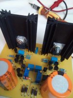
PSU SUCCESS...!
HI..
Finally it started working thank you so much for your support.
Now the output voltage obeys the equation.
Initially I did not connect the 100mfd cap at the output thinking that it is just a decoupling cap and not necessary. Without this cap. the regulator will oscillate and show strange behaviors.
All issues were fixed after connecting the 100mfd cap.
The failure in this project helped me to learn about the functioning of various sections in the schematic.
Now I modified it by replacing 15k with 8.2k to suit to a 12-0-12 transormer.
Its is functioning correctly. Sound is also good.
I remember the words form a Great scientist of our Country Dr. APJ Abdul Kalam
"FAIL: First Attempt In Learning"
Thank you for the news and additional information - sorry to hear about oscillation.
In the original article referenced to in post 3 I wrote that shunt regulators in general
do not tend to parasitic oscillations. It may be different for this example.
In the original article referenced to in post 3 I wrote that shunt regulators in general
do not tend to parasitic oscillations. It may be different for this example.
MOd for high current
Presently,
the current is set by 22R.
Can we reduce it further?
I wish to get 500mA max at 5V for powering a USB MP3 player.
Eqn. for the current limit = (2Vbe)/22R
What are the rules of thumb in selecting the reference voltage?
Could you please detail the functioning if JFET CCS?
Thanks and regards,
Sumesh
Thank you for the news and additional information - sorry to hear about oscillation.
In the original article referenced to in post 3 I wrote that shunt regulators in general
do not tend to parasitic oscillations. It may be different for this example.
In the schematic of post 1: two CCS per side. The operation of these is well known.
For low output voltages and high currents a series regulator is more useful.
For low output voltages and high currents a series regulator is more useful.
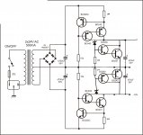
Hi guys. Regarding this +/-18V Shunt PSU, has anyone build it yet? What is the max. load current allowable? Is 500mA too much?
Correct me if I am wrong, but the transistors constitute a constant current source, programmed for 0,7V / 22ohms =~ 31,8 mA. As this is within the serial path, therefore it is not possible for the load to use more than this amount of current, without the regulator falling out of regulation.Hi guys. Regarding this +/-18V Shunt PSU, has anyone build it yet? What is the max. load current allowable? Is 500mA too much?
CCS programmable by the resistor, and subject to Safe Operating Area conditions of transistors and zener diodes.
Due to power limit of the Zener, that needs to dump to ground any excess of current that is NOT consumed by your load, I believe that reaching 500mA with this specific circuit will not be possible.
...
Hey, but what if you "expand the Zener" power-wise, by means of using the Zener (with resistor) as a voltage reference for a high power shunt transistor ? Maybe that would do the trick.
Under no load (i.e. harshest) condition, you would need to "waste" 500mA * 18V = 9W, to be dissipated in the form of heat. A significant radiator / cooling fins will be necessary. Check the SOA of the BD241/BD242 and radiator cooling, if you further explore such a scenario.
Last edited:
Brutal Force + KISS + Fast&Dirty = ...Hi guys. Regarding this +/-18V Shunt PSU, has anyone build it yet? What is the max. load current allowable? Is 500mA too much?
Pls. note:
a). The Zener should be modified by a value of the two Vbe's, that are now introduced into the shunt path; Say, 19,5V.
b). You need to re-program the CCS resistors, to R = 0,7V/ I_max; For assumed I_max, check if SOA conditions are satisfied for the power transistors. Remember about need for thermal de-rating.
c). You need to provide some significant radiators for the serial and shunt power transistors, so that they can dissipate the heat that you shall introduce with I_max.
This is very crude and brutal, but actually ... should work.
Attachments
Last edited:
What is the max. load current allowable? Is 500mA too much?
For low output voltages and high currents a series regulator is more useful.
.. The transistors constitute a constant current source, programmed for 0,7V / 22ohms =~ 31,8 mA. As this is within the serial path, therefore it is not possible for the load to use more than this amount of current, without the regulator falling out of regulation.
Brutal Force + KISS + Fast&Dirty = ...
Pls. note:
a). The Zener should be modified by a value of the two Vbe's, that are now introduced into the shunt path; Say, 19,5V.
b). You need to re-program the CCS resistors, to R = 0,7V/ I_max; For assumed I_max, check if SOA conditions are satisfied for the power transistors. Remember about need for thermal de-rating.
c). You need to provide some significant radiators for the serial and shunt power transistors, so that they can dissipate the heat that you shall introduce with I_max.
This is very crude and brutal, but actually ... should work.
I think your circuit in post 158 should not bear the Apex name.
Position of zeners and 15k resistors has to be reversed (easiest change to make your circuit work).
15k is too high for this use.
Yes, you are right .... it was a quickie cut-copy-paste so as to show the general concept .... indeed, zeners need be transposed with resistors.Position of zeners and 15k resistors has to be reversed (easiest change to make your circuit work).
15k is too high for this use.
Below is a better version.
For 18V output, I suggest that you use a 16V Zener with additional 0,7V diode. Together with two Vbe's:
16V + 3 x 0,7V =~ 18v
Attachments
Last edited:
- Home
- Amplifiers
- Power Supplies
- A-class Preamp PSU