Lessons Learned
Over the past couple of days, I have learned two first-order lessons:
1. Vias are cheap. Use them whenever you need.
2. Layers are cheap (to a certain extent). Don't be afraid to go with 6 layers. It makes everything a lot easier.
I also re-learned a second-order lesson that I already knew but became even more apparent: a board design should be done in an iterative fashion. Of course, we do that already by breaking down the design into two main phases: schematic and PCB. But that's not enough. Once the schematic has been done, a rough PCB design should be done on paper, to make sure that the main constraints can be resolved. Otherwise, a lot of EDA time might go to waste...
And this is especially important for boards that deal with user interfaces, because these have very strong mechanical constraints, and dealing with the interplay between mechanical and electrical constraints is where the challenge lies.
Also, I have a much better appreciation for two things:
1. Parts should be selected very, very carefully.
2. Components should be added only when absolutely necessary.
Unlike software features, hardware features are really expensive and have a lot of side effects. Therefore, before adding a feature, one should seriously consider whether the feature is absolutely necessary or not. And if it is not, it should be discarded.
In other words, it's all about learning how to say "No!"
Last edited:
Unintended Consequences
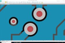
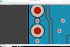
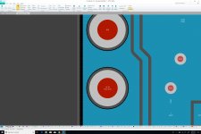
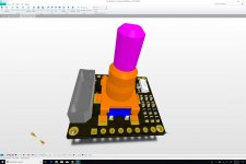
Here is a great example of the interplay between seemingly unrelated mechanical constraints: yesterday, we found a way to center the rotary encoder on our board. This was great, because it made it super easy to center the encoder on the brick itself, both horizontally and vertically. But this came with a totally-unintended consequence: it reduced the maximum diameter of our LED ring. Let me explain why.
As you can see on this screenshot, there is not a lot of space between the Hirose connector for the mezzanine board on which the LEDs will be mounted and the shaft of the rotary encoder. In our previous design, the encoder was rotated by 90 degrees and was mounted further away from the Hirose connector. But when trying to center it on the board, we had to mount it in a rotated fashion, and we had to bring it as close as possible to the mezzanine connector. At first, this seemed like a great idea.
Unfortunately, we later realized that it would come at a cost: the Hirose receptacle on the base board has to be matched by an Hirose plug on the mezzanine board, and this plug will itself be quite close to the encoder's shaft. As a result, the space we have for our LED ring between the connector and the encoder will be quite limited, and it certainly won't allow us to use as large a knob cap as we expected.
Fortunately, this does not seem to be a deal breaker: all we'll have to do is push our LEDs as close to the Hirose connector as possible, and settle on slightly smaller knobs. But this is a good lesson for the future: whenever we make an Engineering Change Order, we should give very serious thoughts to all its side effects, be they electrical, mechanical, or financial.
Engineering 101...
Attachments
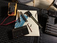
When you get there to order the pcb, you will certainly need to generate Gerber format output files.
Check those files with an external viewer tool (like freeware : "gerbv").
Note: internal plane layers usually come in negative (inverse) in gerbers. If you use internal planes, use them only for power, don't use it for any routing!
Check those files with an external viewer tool (like freeware : "gerbv").
Note: internal plane layers usually come in negative (inverse) in gerbers. If you use internal planes, use them only for power, don't use it for any routing!
When you get there to order the pcb, you will certainly need to generate Gerber format output files.
Check those files with an external viewer tool (like freeware : "gerbv").
Note: internal plane layers usually come in negative (inverse) in gerbers. If you use internal planes, use them only for power, don't use it for any routing!
Yes, of course. I am using internal planes only for VCC, 3V3, and GND.
Thanks a lot for the heads up though, much appreciated!

Power Supply for DAC
Frex has done some measurements for his AAPSU01v1 power supply, and they look excellent. Therefore, I confirm that we will implement his design for the power supply of our DAC.
Frex has done some measurements for his AAPSU01v1 power supply, and they look excellent. Therefore, I confirm that we will implement his design for the power supply of our DAC.
Last edited:
...we will implement his design for the power supply of our DAC.
Wouldn't quite go that far, myself. Probably be more inclined to say, 'we will perform listening tests with the power supply as final verification of its suitability for use with the dac.'
High end audio design should include both measurements and listening tests. Only doing one or the other isn't enough.
I think you're right, I'm getting carried away. Just happy to know that we have a good option that we can start from.
Problem with LEDs
Bad news: the reverse-mounted LEDs that we were planning to use won't fit within our current design. They're simply way too big compared to the ones used by the Knob G Click. So we're back to the drawing board...
Bad news: the reverse-mounted LEDs that we were planning to use won't fit within our current design. They're simply way too big compared to the ones used by the Knob G Click. So we're back to the drawing board...
Bad news: the reverse-mounted LEDs that we were planning to use won't fit within our current design. They're simply way too big compared to the ones used by the Knob G Click. So we're back to the drawing board...
We will probably take advantage of this setback to improve the overall design based on the very many lessons that we have learned.
First, we will most likely abandon the mikroBUS form factor, while keeping its electrical interface. This decision is motivated by the fact that we've already deviated quite a bit from the original specification, both mechanically and visually. Also, as mentioned in earlier posts, we need some additional circuits for 12V power and I²S. Therefore, we might as well define our own interconnect. And we will use surface mounted connectors instead of through hole 2.54mm headers. These will be easier to assemble at the fab, they will give us a much lower profile, and they will make the mounting/unmounting of bricks on the plate much easier for the end-user. While mikroBUS is using 2 sets of 8 pins, we will probably use 2 sets of 12 or 16 pins, leaving a handful of pins available for future enhancements.
Second, we will make our board perfectly square (28mm × 28mm). This will make the assembly within a 32mm × 32mm frame a lot more convenient than the rectangle footprint used by mikroBUS boards.
Third, we will remove the voltage selector. It is making the overall circuit a lot more complex than it should be, and it will allow us to move back to a 4-layer design. VCC = +3.3V, and that's it...
Fourth, we will go from two to three PCBs for the E1 brick:
1. Encoder board
2. LED board
3. Cover board
By doing so, we will be able to use standard LEDs (not the reverse-mount kind), and the cover board will be free of any through hole.
Fifth, we will take advantage of our slightly larger form factor in order to use more conventional fastening hardware (M2 ideally).
Let's go!
Wouldn't quite go that far, myself. Probably be more inclined to say, 'we will perform listening tests with the power supply as final verification of its suitability for use with the dac.'
High end audio design should include both measurements and listening tests. Only doing one or the other isn't enough.
Disclaimer being that this is your opinion and not fact. 🙂
We will probably take advantage of this setback to improve the overall design based on the very many lessons that we have learned.
First, we will most likely abandon the mikroBUS form factor, while keeping its electrical interface. This decision is motivated by the fact that we've already deviated quite a bit from the original specification, both mechanically and visually. Also, as mentioned in earlier posts, we need some additional circuits for 12V power and I²S. Therefore, we might as well define our own interconnect. And we will use surface mounted connectors instead of through hole 2.54mm headers. These will be easier to assemble at the fab, they will give us a much lower profile, and they will make the mounting/unmounting of bricks on the plate much easier for the end-user. While mikroBUS is using 2 sets of 8 pins, we will probably use 2 sets of 12 or 16 pins, leaving a handful of pins available for future enhancements.
Second, we will make our board perfectly square (28mm × 28mm). This will make the assembly within a 32mm × 32mm frame a lot more convenient than the rectangle footprint used by mikroBUS boards.
Third, we will remove the voltage selector. It is making the overall circuit a lot more complex than it should be, and it will allow us to move back to a 4-layer design. VCC = +3.3V, and that's it...
Fourth, we will go from two to three PCBs for the E1 brick:
1. Encoder board
2. LED board
3. Cover board
By doing so, we will be able to use standard LEDs (not the reverse-mount kind), and the cover board will be free of any through hole.
Fifth, we will take advantage of our slightly larger form factor in order to use more conventional fastening hardware (M2 ideally).
Let's go!
That seems like a better approach. Are you going to make a light pipe or something for the LEDs or just clear the cover PCB?
That seems like a better approach. Are you going to make a light pipe or something for the LEDs or just clear the cover PCB?
Thanks for the feedback, much appreciated.
Regarding the cover PCB, I was thinking of keeping it clear alongside a ring line. I could also "simulate" light pipes by having something like 4 planes of copper and making 24 openings in the copper on each layer. This would allow light to be "funneled" through these 24 sets of four openings aligned with the underlying LEDs that are mounted on the middle PCB.
32 RGB LEDs
Since we're going to redesign our E1 brick, we might as well consider improving the LED ring. One problem with the original design is that it is using single-color LEDs, and there are many applications for which RGB LEDs would be much more appropriate. Also, by going from 24 LEDs to 32 LEDs, we would improve the "continuity" of our LED ring by 33%. Therefore, I am considering using two TLC5958 48-channel LED drivers and small RGB LEDs from SunLED (either XZxxxxxx158W or XZxxxxxx62W-2). Before we commit to anything though, we'll make sure that we have enough room for all this...
Since we're going to redesign our E1 brick, we might as well consider improving the LED ring. One problem with the original design is that it is using single-color LEDs, and there are many applications for which RGB LEDs would be much more appropriate. Also, by going from 24 LEDs to 32 LEDs, we would improve the "continuity" of our LED ring by 33%. Therefore, I am considering using two TLC5958 48-channel LED drivers and small RGB LEDs from SunLED (either XZxxxxxx158W or XZxxxxxx62W-2). Before we commit to anything though, we'll make sure that we have enough room for all this...
Separating the Encoder from the LED Ring
With the new design, we might want to move the LED driver(s) from the encoder board to the LED board. This would have the advantage of making the LED ring optional (some applications might not need it). It would also make it possible to use connectors with much less circuits between the two boards. In fact, I am starting to think that the two boards should use the same interconnect as the one used between the brick and the plate (what we're going to call the "OTO" interconnect). And the same interconnect could be used between the LED board and the cover board, even though the cover board might not have any component on it.
With the new design, we might want to move the LED driver(s) from the encoder board to the LED board. This would have the advantage of making the LED ring optional (some applications might not need it). It would also make it possible to use connectors with much less circuits between the two boards. In fact, I am starting to think that the two boards should use the same interconnect as the one used between the brick and the plate (what we're going to call the "OTO" interconnect). And the same interconnect could be used between the LED board and the cover board, even though the cover board might not have any component on it.
- Home
- Source & Line
- Digital Line Level
- 8 × AK5578EN + 8 × AK4499EQ ADC/DAC Boards