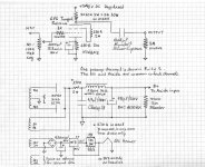
Voltage reg is based on Vref too. Just on a resistors divider. When it works as a voltage reg it also can work as a CCS.

Mosfet cap multiplier PSU board done, more or less. It has a CRC filter before the feed to the mosfet to help burn up a little ripple and pad the charging inrush of the caps. Very happy with how this turned out so far! Looks like a great, simple companion board to the 6V6 PCBs, and should be super handy for lots of tube projects in the future.

Gonna work on a Maida next. It'll be double the size but will share a lot of the same layout, should make for an easy build up and comparison. The mosfet cap multiplier PCB is 50x50mm, Maida board will be twice as wide at 50x100mm.
Gonna work on a Maida next. It'll be double the size but will share a lot of the same layout, should make for an easy build up and comparison. The mosfet cap multiplier PCB is 50x50mm, Maida board will be twice as wide at 50x100mm.
Last edited:
C3 and C4 are overlapping ZD1... You probably want to move them up/down one step. 🙂
Also, mounting diodes and resistors vertically makes a much smaller board 🙂
I just made this board for a depletion MOSFET gain stage to try and replace a 6SN7... Imagine how much bigger the board would have been without vertical parts? 😀

Also, mounting diodes and resistors vertically makes a much smaller board 🙂
I just made this board for a depletion MOSFET gain stage to try and replace a 6SN7... Imagine how much bigger the board would have been without vertical parts? 😀
I don't know why but I'm not a fan of vertical mounting, maybe it's just a preference thing. I'm still within the 50x50mm goal so I'm happy with everything being laydown. I also find it easier to populate with everything flat too. Maybe on another build I'll try vertical just to get used to it?
I just looked at the zener pads as you state, I can scoot things around a bit to give them more room, it'll look cleaner. Don't know how I glossed over it.
Ay, what heatsink are those footprints for? Those look handy.
I just looked at the zener pads as you state, I can scoot things around a bit to give them more room, it'll look cleaner. Don't know how I glossed over it.
Ay, what heatsink are those footprints for? Those look handy.
The heatsink footprints are for these ones... They go on the IXTP08N100D2 MOSFETs... I just build up a board to test it. There are two resistors missing because I don't know what value they should be yet 🙂
I guess I should have wiped the goop off of the heatsink before I took the photo LOL

I guess I should have wiped the goop off of the heatsink before I took the photo LOL
Good luck. Do you have a way to build and test one outside of the amp to verify function?
Keep in mind that the mounting tab is tied to the output (pin 2) and needs to be isolated when attached to a heatsink, it cannot be tied to ground.
Keep in mind that the mounting tab is tied to the output (pin 2) and needs to be isolated when attached to a heatsink, it cannot be tied to ground.
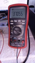
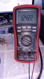

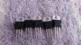
What is the actual measured supply voltage (Vcc) to the LM317? you want at least 4-5 volts or so headroom or the output will be low and act strange. For 6.3 volts out I would want at least 10 volts or more to give room for regulation.
Are you putting the LM317 on the high side of the circuit, between the supply voltage and the filament, or low side of the circuit between filament and ground?
For troubleshooting, I like putting them on the low side, because it makes the wiring easy-
-ground the ADJ pin (pin 1)
-resistor goes between OUT (pin 2) and ground
-one end of filament goes to IN (pin 3)
-one end of filament goes to Vcc/supply voltage
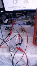
A good idea also would be to check that the socket has no solder splash shorts or debris bridging the terminals.
Are you putting the LM317 on the high side of the circuit, between the supply voltage and the filament, or low side of the circuit between filament and ground?
For troubleshooting, I like putting them on the low side, because it makes the wiring easy-
-ground the ADJ pin (pin 1)
-resistor goes between OUT (pin 2) and ground
-one end of filament goes to IN (pin 3)
-one end of filament goes to Vcc/supply voltage
A good idea also would be to check that the socket has no solder splash shorts or debris bridging the terminals.
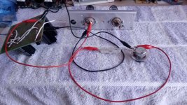
what are you getting after rectification of the 9VAC? are you using a set of four diodes as a bridge or a single bridge?
Please post some pics and measured voltages. That way we can start from the very beginning and go step by step.
If you have that voltage on pin 1 that is the ADJ pin, pin 3 is the IN pin and should have the Vcc on it.
- Home
- Amplifiers
- Tubes / Valves
- 6V6 line preamp