Graham Maynard said:The posts have come in quickly here.
Sajti, you asked about combining 'B' and 'C'.
I do not see 'B' as maintaining class-A operation.
At moments when load current demand increases drive such that a CCS fed VAS can cut off, then so too will drive conduction through the common emitter resistor(s).
Your post #35 circuit does not show the drive or biasing, but it is bound to have a good safety margin for output current.
Cheers ........... Graham.
Hi Graham,
I mean that the driver and the predriver run in class A in the version B. Off course, properly designed VAS necessary, but it necessary for all the 3 version. But my experience is that 3-5mA bias is enough with 3 deep darlington.
sajti
Hi Sajti,
I still do not see 'B' maintaining class-A pre/driver operation at all times.
Most of the time maybe, but I can see the possibility for momentarily harsh sounding high level reproduction.
At maximum output, with say a CCS pulling Q1 up and the VAS off, Q4 carrier/charge might well be capable of momentarily reverse biasing Q5 when voltage is dropped by R3, because Q6/Q5 bias is not referenced to the Q4 emitter resistor.
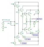
Unfortunately my thoughts for possibility are not good enough, so I have simulated the driver current using this circuit.
I am also surprised to see pre-driver crossover spiking.
Both the spiking and 'non-class-A' current dropout will have audible impact at these instants.
Cheers ........... Graham.
I still do not see 'B' maintaining class-A pre/driver operation at all times.
Most of the time maybe, but I can see the possibility for momentarily harsh sounding high level reproduction.
At maximum output, with say a CCS pulling Q1 up and the VAS off, Q4 carrier/charge might well be capable of momentarily reverse biasing Q5 when voltage is dropped by R3, because Q6/Q5 bias is not referenced to the Q4 emitter resistor.
Unfortunately my thoughts for possibility are not good enough, so I have simulated the driver current using this circuit.
I am also surprised to see pre-driver crossover spiking.
Both the spiking and 'non-class-A' current dropout will have audible impact at these instants.
Cheers ........... Graham.
Attachments
I think that all 3 types are potentially useful. I would have to do an extensive Spice simulation of each, (all else being equal in the semiconductor operating conditions) to see the advantages and disadvantages of each. I have used both A and B with good results, but C looks OK as well, perhaps, maybe even better in some conditions.
Hi All,
I think the choice relates to individual requirements, and whether one accepts different types of overall closed loop stability regimes.
The circuit by mfc might similarly have its uses, but it introduces additional phase change when compared to those originally being discussed.
Cheers............ Graham.
Graham Maynard said:Hi Sajti,
I still do not see 'B' maintaining class-A pre/driver operation at all times.
Most of the time maybe, but I can see the possibility for momentarily harsh sounding high level reproduction.
At maximum output, with say a CCS pulling Q1 up and the VAS off, Q4 carrier/charge might well be capable of momentarily reverse biasing Q5 when voltage is dropped by R3, because Q6/Q5 bias is not referenced to the Q4 emitter resistor.
Unfortunately my thoughts for possibility are not good enough, so I have simulated the driver current using this circuit.
I am also surprised to see pre-driver crossover spiking.
Both the spiking and 'non-class-A' current dropout will have audible impact at these instants.
Cheers ........... Graham.
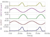
Your results quite interesting! Unfortunately You not labelled the parts, so I'm not sure which is which 😕 It also interesting how the capacitors across the emitter resistors change the result. Another question: How much bias current necessary for the drivers to keep them in class A?
sajti
Hi Sajti.
The parts are labelled, semiconductor numbers abbreviated.
It is as much a carrier build up as capacitance in the base region that causes this.
I believe that Michael was broaching this aspect (post#25) in his response to PB2.
Floating resistors cannot (nor the parallel capacitor) guarantee permanent class-A operation, especially with the likes of high energy cymbals driving a crossover/dynamic LS system when the output voltage and current phase can become so far out of phase.
Cheers ........... Graham.
Graham Maynard said:Hi Sajti.
The parts are labelled, semiconductor numbers abbreviated.
Cheers ........... Graham.
I mean Q1, Q2, Q3 etc... The types are OK.
sajti
Hi Sajti,
Oh I see what you mean now.
It seems you expected me to number every component.
*My simulator does not lend itself to doing this easily or clearly* and I am amazed that you make such a petty point.
It is not a circuit diagram, but something I took the trouble to model on your behalf in relation to your statement !!!
Cheers ........ Graham.
Graham Maynard said:Hi Sajti,
Oh I see what you mean now.
It seems you expected me to number every component.
*My simulator does not lend itself to doing this easily or clearly* and I am amazed that you make such a petty point.
It is not a circuit diagram, but something I took the trouble to model on your behalf in relation to your statement !!!
Cheers ........ Graham.
I just want to be sure, that which is which, to follow Your explanation.
sajti
Graham Maynard said:Hi All,
...it introduces additional phase change when compared to those originally being discussed.
Hi,
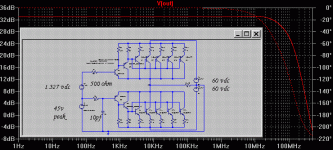
A magnitude phase plot of the attached circuit (and the one
from the previous post) gives a phase shift of the following:
-1.34 degrees at 1Mhz
-.141 degrees at 100Khz
-.0282 degrees at 20Khz
-.0141 degrees at 10Khz
this looks really good, and I would think it compares well
with the other 3 circuits, AFAIK.
Mike
Attachments
jaycee said:Type B is the "Triple Darlington" stage used in the Leach Amp. Both the predriver and driver transistors run in Class A (IE they never turn off thus reducing crossover distortion).
Actually, only the first of the cascaded drivers may be easily persuaded to operate in class A....assuming a class B biased output stage....
In fact, the closed loop performance of the 'type B' circuit is superior to anything out there....
Graham Maynard said:I do not see 'B' as maintaining class-A operation.
The first pair of complementary drivers can easily operate in class-A, even with the output devices biased for class-B operation...
Graham Maynard said:At moments when load current demand increases drive such that a CCS fed VAS can cut off, then so too will drive conduction through the common emitter resistor(s).
Well then, the amp. could not be said to operate in its linear region in these circumstances....
cutting off an active current source can only mean its compliance has been infringed....
which only occurs when the amp. is driven to clip....
....the class of operation of the drivers (or indeed any stage of the design) in these circumstances becomes entirely academic....
Graham Maynard said:Hi Sajti,
I still do not see 'B' maintaining class-A pre/driver operation at all times.
Graham Maynard said:And the Current/Voltage simulations.
Graham,
Actually your simulation shows that each member of the first pair of drivers conducts throughout the cycle...
Which proves class-A operation......
As I checked the simulation made by Graham, I found the following:
The output drivers are not working in class A all the times, if I drive my amplifier to the clipping, with 20kHz sine wave, AND I set low bias for the drivers.
To get class A operation every time, I have to set the bias high enough, to charge/discharge the input capacitance of the output transistors. This means, that 100-200mA bias for the drivers are not too much. I checked the Mark Levinson 23.5 amplifier. It use 3paralleled MJEs to drive 8 MJ15024s. And the bias is about 150mA for the drivers, and about 30mA for the predrivers...
The crossover spiking in the predriver stage resulted by the switch on/off of the drivers. So if I set higher current for the drivers, and avoid the switch off, there will be no problem with the predrivers.
sajti
Hi everyone
Hi everyone,
We bias the drivers at 100mA [total Class-A operation] , just to drive the vertical mosfets only!.😀
In case of our IGBT amp , the drivers are biased at 200mA to ensure EXTRA hard punching bass +++ lots of damping factor.😉
Cheers,
Kanwar
Hi everyone,
We bias the drivers at 100mA [total Class-A operation] , just to drive the vertical mosfets only!.😀
In case of our IGBT amp , the drivers are biased at 200mA to ensure EXTRA hard punching bass +++ lots of damping factor.😉
Cheers,
Kanwar
K-amps said:Satji,
Mind sharing the schematic of the 23.5? thanks in advance!
I got the schematics from this forum 😎 Try to do some search, because I don't remember which topic contains them.
Very complicated design anyway, with lot of devices...
sajti
sajti said:As I checked the simulation made by Graham, I found the following:
The output drivers are not working in class A all the times, if I drive my amplifier to the clipping, with 20kHz sine wave, AND I set low bias for the drivers.
To get class A operation every time, I have to set the bias high enough, to charge/discharge the input capacitance of the output transistors. sajti
Hi Sajti,
To obtain class A operation in the first pair of drivers, all you have to do is:
1) Ensure that the output devices are at least biased for 'optimal' class B..(i.e:not underbiased!)...class AB for the output devices is much better...contrary to D. Self.
Do not underbias...as the first pair of drivers in this scheme tend to burst into sporadic oscillation at crossover...
2) Have a sufficiently small cross-coupling resistor for the first pair of drivers (typically less than 1K)
Hi, Mikeks,
In some design, I found B circuit with RE of 0.22ohm/5W or 0.1ohm, but it has diode -forward bias position- parrarel to it. The biasing scheme is VBE multiplier. I assume this is for limiting maximum drop in 0.22ohm resistor to 0.6V (=forward diode) at bigger output current.
What is really the purpose of this diode parrarel with RE? To make Xover-distortion better?
- Status
- Not open for further replies.
- Home
- Amplifiers
- Solid State
- 3 Different Outputstage Driver Arrangements, Your Opinions!