My aim was never "Class A" as such, but very good performance from a simple amplifier. And below class A setting, the point just below 400mA is working very well indeed!
See this thread for more info (post #12):
http://www.diyaudio.com/forums/solid-state/31420-what-quiescent-current-hitachi-2sk1058-2sj162.html
See this thread for more info (post #12):
http://www.diyaudio.com/forums/solid-state/31420-what-quiescent-current-hitachi-2sk1058-2sj162.html
I'm afraid that direct comparison is not possible because usual vertical suspects (IRFP9240/240) will go wild without Source resistors and using them eliminates square law advantage. . . . .
Perhaps IRF9530N/630N can be used on 24V, probably up to 32V supply. Have positive result on modified F5 at +-12V and 500mA without source degeneration.
Sorry, but my scope (and the sim for that matter) shows the same thing as Mr. Pass' paper does. Also, check the post #41 of this thread.
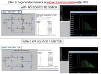
So, there is a clear class A extended region in the common Drain (Source follower) mode:
as promised i did some work on this and contrary to my previous post - you are correct, we do see the effect in follower stages. Apologies for any confusion that I may have caused 😱
As penance for my mistake, i present the comparisons below - that should (hopefully) go some way in convincing Andrew. Note that the op stages are all operated deliberately outside the 2*Iq rule to show that that this effect is due to a larger class A region.....
Attachments
This amplifier is really amazing....the idea was to have a nice "in between" amplifier, but it seems it is stuck inside my main system...nothing seems to be able to up it 🙂
But I have a need for at little more gain on old recordings---a few dB (3-6). Can I cange R13 or R2 without sonic trouble?
My guess is R2....
But I have a need for at little more gain on old recordings---a few dB (3-6). Can I cange R13 or R2 without sonic trouble?
My guess is R2....
Good guess ! 🙂...My guess is R2....
Solder another 1k resistor parallel to R2 and you'll have 6db gain more. After you do it, check/reset Iq (P2) and half +V at the output (P1).
There'll be no "sonic trouble" but some minor change is to be expected - alone the fact that the amp will play louder will change the listener's perception...
Good guess ! 🙂
Solder another 1k resistor parallel to R2 and you'll have 6db gain more. After you do it, check/reset Iq (P2) and half +V at the output (P1).
There'll be no "sonic trouble" but some minor change is to be expected - alone the fact that the amp will play louder will change the listener's perception...
Thank you 🙂
Good guess ! 🙂
Solder another 1k resistor parallel to R2 and you'll have 6db gain more. After you do it, check/reset Iq (P2) and half +V at the output (P1).
There'll be no "sonic trouble" but some minor change is to be expected - alone the fact that the amp will play louder will change the listener's perception...
Working perfectly 🙂
I stumpled over an application note:
http://www.ti.com/lit/an/snaa045a/snaa045a.pdf
In section 9.1 the measure the optimal gate resistors for 1058/162 and found them to be 190-210R/240-330R.
My calculations and actual values used are the changed: R16=220R and R17=330R, giving a Ft og aprox. 800kHz...
😕
Measured, calculated, simulated ?
Just calcualted from Ciss: 600pF and 900pF...giving 220R and 330R...
I was just wondering why the application notes testing in actual Circuit came to the switched results?
I wouldn't dwell too much on the subject. It's easy to change gate stoppers in 50R - 1k range and see for yourself what change does it bring - I won't tell you about my findings to avoid influencing your conclusions 😉
Ok, I will rest...I don't have stability issues so I will leave the 220R-2SK1058 and 330R-SJ162 in Circuit 🙂
I'm afraid that direct comparison is not possible because usual vertical suspects (IRFP9240/240) will go wild without Source resistors and using them eliminates square law advantage.
There are ways to get around that - for example, see the F6 amplifier, where the drive
circuit allows both square law character and Source resistors.
😎
Dear Juma man,
I've read hundreds of times, and it is still not clear to me: We keep source resistors until we set-up quiescent current, and when set it, we remove resistors (short em up)?
Other than that, I have designed some PCB, wanted to put it all onto PCB (to avoid wires, wires, wires...), so if you can see something wrong with it, please point at it 🙂
Alex
I've read hundreds of times, and it is still not clear to me: We keep source resistors until we set-up quiescent current, and when set it, we remove resistors (short em up)?
Other than that, I have designed some PCB, wanted to put it all onto PCB (to avoid wires, wires, wires...), so if you can see something wrong with it, please point at it 🙂
An externally hosted image should be here but it was not working when we last tested it.
Alex
... We keep source resistors until we set-up quiescent current, and when set it, we remove resistors (short em up)?...
Yes. With only one pair of output MOSFETs, the 0R1 resistors serve only for convenient Id measurement. If you need to drive very low impedance load into high signal levels you might need another pair of outputs - in that case, keep those resistors in the circuit.
I'm bad at checking other peoples PCB layouts, you'll have to do it yourself. 🙂
Hint: grey on black is not making it easier, but even in such a low contrast pic I see mixed up D and S on 2sk1058...
Hagh - I used this guy's Eagle library: http://www.diyaudio.com/forums/software-tools/195440-eagle-lateral-fet-models.html#post3690992 so it's wrong set there...
Now fixed, and right channel displayed 🙂
(if anyone is interested in Eagle layout files, please PM)
Now fixed, and right channel displayed 🙂
An externally hosted image should be here but it was not working when we last tested it.
An externally hosted image should be here but it was not working when we last tested it.
(if anyone is interested in Eagle layout files, please PM)
A couple things I would change on this PCB:
- ground layout; I'd separate the small signal ground traces from the power ground traces then join them in a star ground at the end; I think your input ground connection will cause a ground loop scenario;
- traces to the filter caps, eg. C3; I wouldn't make a single trace to C3, but one going to it and one leaving to Q3; there's this recommendation that you do not take the power from a point between a rectifier bridge and reservoir cap, but from the cap; same principle applies; I always separate the trace that is charging the capacitor from that which discharges it.
Do not consider your traces as zero ohm resistances. Plan your circuit as if your traces would have a considerable resistance and imagine what happens when large currents go trough them.
Thanks ceteras. To be honest, I was thinking the same for ground loop and star gnd, but thought maybe I could here get through without it 😀
So here are the two new layouts:
http://i318.photobucket.com/albums/mm404/acamilicko/SV_L_zps4e7e6716.png
http://i318.photobucket.com/albums/mm404/acamilicko/SV_R_zps983a152a.png
😎
So here are the two new layouts:
http://i318.photobucket.com/albums/mm404/acamilicko/SV_L_zps4e7e6716.png
http://i318.photobucket.com/albums/mm404/acamilicko/SV_R_zps983a152a.png
😎
This looks a lot better . I like how you've changed R8 and R10 resistors' position too.
You could align them, place R8 right beneath R10, then C5 and R21 too. Things look better when aligned.
Can you turn C7 with its negative up, route its ground connection beneath R33, then the link from R23 to C8 beneath C7 and straight to +C8?
Or perhaps you could move all the ground line from C15 to R12 beneath those components and link it to the input ground line. This could help with the line from R21 to Q1, make it prettier.
Just another 50 cents.
- Home
- Amplifiers
- Pass Labs
- 25W Class A amp with Lateral MOSFETs