
It should work.
LATFET's source resistors are there only for convenient bias setting - in normal operation they are short-circuited (see post #1).
LATFET's source resistors are there only for convenient bias setting - in normal operation they are short-circuited (see post #1).
Thanks juma.
One more question.
If I have to insert a ground lift, would it be between grounds of input -ve , C15, C7, C14, R23? Related question, would ground lift work here and be beneficial?
Yes, I know about source resistor removal after bias setting. So I have kept 2 pairs of pads for source resistors, so user can simply put a jumper across a pair of pads and be done with it. He can leave source resistor in place for trials with different bias settings and SQ and temperature tolerance of his build (Bias from 400mA to 1.3 A as recommended by you, for winter 😉).
Regards
Prasi
Last edited:
Only 'dirty' gnd here is at first filter cap after the bridge. So if there is no loop, no need for ground lift.
Prasi,
I would put a 10 ohm resistor between X1-2 and the GND. It is impossible to predict that the output of any ancillary equipment could not cause a ground loop.
I would put a 10 ohm resistor between X1-2 and the GND. It is impossible to predict that the output of any ancillary equipment could not cause a ground loop.
They are both single rail, simple circuits that use the same output stage and PSU - very easy to try for your self and decide what you prefer...
Prasi,
I would put a 10 ohm resistor between X1-2 and the GND. It is impossible to predict that the output of any ancillary equipment could not cause a ground loop.
Hi Nico,
Thank you for your comment.
Good thing that AndrewT is not around (since beginning of Feb), other wise he would be all over you with this😀...
https://www.updatemydynaco.com/documents/GroundingProblemsRev1p4.pdf
regards
Prasi
Some ideas
Hello Prasi,
nice layout for a nice class A amp.
As juma already mentioned, the source resistors are nice to have for setting the bias comfortable.
Here a few suggestions for modification:
- Could you please move all FET in that way, that their cases don't prolude from the board outline, means moving them towards the center of the pcb.
- for fixing the FETs on the heatsink a drilled hole with 6,3mm diameter on the pcb would be helpful.
- if possible length should be < 100mm for one side
- if you plan to publish the layout, please all drill holes as double sided met. vias.
- maybe an measurement resistor in the supply rail for setting the bias, and then shorting the resistor for operation.
Thanks in advance
Günni
PS : i 'm interested, since a LATMOSFET amp in Class A is not in my collection 😉
Hello Juma,
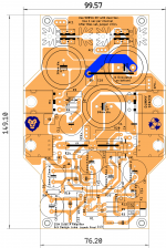
Here is a diy friendly layout of your amp.
Could you take a look at grounding and tell me if its ok?
regards
Prasi
Hello Prasi,
nice layout for a nice class A amp.
As juma already mentioned, the source resistors are nice to have for setting the bias comfortable.
Here a few suggestions for modification:
- Could you please move all FET in that way, that their cases don't prolude from the board outline, means moving them towards the center of the pcb.
- for fixing the FETs on the heatsink a drilled hole with 6,3mm diameter on the pcb would be helpful.
- if possible length should be < 100mm for one side
- if you plan to publish the layout, please all drill holes as double sided met. vias.
- maybe an measurement resistor in the supply rail for setting the bias, and then shorting the resistor for operation.
Thanks in advance
Günni
PS : i 'm interested, since a LATMOSFET amp in Class A is not in my collection 😉
It should work.
LATFET's source resistors are there only for convenient bias setting - in normal operation they are short-circuited (see post #1).
Hello Prasi,
nice layout for a nice class A amp.
As juma already mentioned, the source resistors are nice to have for setting the bias comfortable.
Here a few suggestions for modification:
- Could you please move all FET in that way, that their cases don't prolude from the board outline, means moving them towards the center of the pcb.
- for fixing the FETs on the heatsink a drilled hole with 6,3mm diameter on the pcb would be helpful.
- if possible length should be < 100mm for one side
- if you plan to publish the layout, please all drill holes as double sided met. vias.
- maybe an measurement resistor in the supply rail for setting the bias, and then shorting the resistor for operation.
Thanks in advance
Günni
PS : i 'm interested, since a LATMOSFET amp in Class A is not in my collection 😉
Hello Günni,
Thank you.
Due to some other work at present I am not able to incorporate all your suggestions in the layout.
However as a quick solution, I have made following layout.
1. I have the fets mounted under the PCB. If you decide to manufacture double sided PCB, I have given a trace on top side instead of the jumper meant for single sided layout. I will print PTH and vias in the gerbers , no problem.
2. 6.3 dia hole on PCB is provided for mounting the fets.
3. Note the dummy fet on the right, it is just to stabilize, so you can avoid corner mounting holes all together.
4. component options are not very premium, but run of the mill Wima PP caps could be found. I can provide the used capacitor dimensions (BoM), you could check if its suitable for your requirement.
5. width <100mm.
let me know if you are still interested.
regards
Prasi
Attachments
Last edited:
Hello Juma,
Here is a diy friendly layout of your amp.
Could you take a look at grounding and tell me if its ok?
regards
Prasi
Dear Juma,
As per your advice, I was looking around for a suitable layout for your amp and lo, Prasi published this.
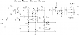
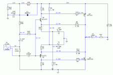
In your circuit for 5 to 10 watt amp, attached below, you used a different arrangement to get mid point biasing of input transistors. Can it be used here also as it will save one Elco? Also, do you recommend using D1, input RF filter R18 and C6 here also ? Any recommendation for output Zobel and Choke ?
Dear Prasi, Depending on the advice of Juma, you may do modifications as suggested. You may include place holders for GS protection Zenar-Diodes for those that may have to use different Laterals than specified.
--Sarma.
Attachments
NoCan it be used here also as it will save one Elco?
No need for that but you are free to try whatever you like...Also, do you recommend using D1, input RF filter R18 and C6 here also ? Any recommendation for output Zobel and Choke ?
Hi Prasi,
thanks for the modifications so far.
Wouldn't it be better to keep the rectangular format of the pcb with width < 100mm, and do not cutouts? Maybe it's then possible to use 35 mm diameter capaictors for the big ones. I think it's hard to find them with 30mm diameter in the requested capacities.
wouldn't it be safer for the MOSFETs to build in some protection diodes between gate and source. Otherwise the layout looks very promising.
Still intersested in this design
best regards
Günni
If you look at the Hitachi/Renesas datasheets for k135/j50 and k1058/j162, you'll see that they already did it ....... wouldn't it be safer for the MOSFETs to build in some protection diodes between gate and source....
Hi Juma,
I am also not able to access the various links. Could you please post a BoM for your "Therapy" amp, as well as any gerbers that may be availabe? I'm quite keen to do a layout myself - as a practice run. I'm a reasonable newbie to electronics.
Regards, Kevin
I am also not able to access the various links. Could you please post a BoM for your "Therapy" amp, as well as any gerbers that may be availabe? I'm quite keen to do a layout myself - as a practice run. I'm a reasonable newbie to electronics.
Regards, Kevin
Sorry Ferret, I got no BOM as such.
The schematic (post #1 of this thread) is simple enough and shows all needed parts - all capacitors should be 63V rated (or more if you like).
The schematic (post #1 of this thread) is simple enough and shows all needed parts - all capacitors should be 63V rated (or more if you like).
Hi Juma ,Wow, Sam ! That's some review ! 😀
F5 with k2013/j313 is, as I already said, the end of the road when it comes to 20W cl. A amps (that's my opinion).
But this time I wanted something that doesn't have to be perfect in every possible aspect, but it has to be always pretty and attractive without being wrong.
For example: listening to MP3 through F5 is not a pleasent experience, with this amp it's far more enjoyable. Not all our sound sources are perfect, I use the amp to listen to TV and FM tuner too - and I want to enjoy it too. 🙂
Could you please give some more info about the differences between them , as what does it mean by one being perfect in all aspects and other being attractive and pretty without being wrong ?
Is it the differences in harmonic contents ??
What makes it sound better irrespective of quality of the source and speakers? Could you please tell how does MP3 sound good on one and not on other ..
- Home
- Amplifiers
- Pass Labs
- 25W Class A amp with Lateral MOSFETs