Finally all boards are here. There was some complication with fabrication. First delivery of the amp boards have some errors in the soldering mask, and after my complain they admitted it was a fault in the production and shipped new correct boards with discount.
Here is the previous list of order:
platon.rado-6 pieces/only power amp pcb/
Cambe- 2 Amp PCB's and 2 Reg PCB's.
Ajit- 2 Amp PCB's and 1 reg pcb
ejno - 2 amp PCB's and 2 Reg PCB's
vac231 - 2 amp PCB's and 2 Reg PCB'
Joshvi- 2 Amp PCB's and 1 reg pcb
I have now more pcbs to offer, 20 amp boards with no soldering mask errors for 19 EURO + shipping, more then 20 amp boards with the soldering mask errors(easy to rectifier by rub off some protective paint) for 13 EURO + shipping and 10 PS Regulator boards for 19 EURO + shipping.
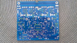
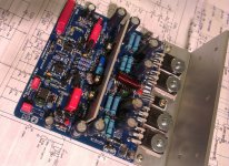
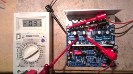
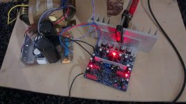
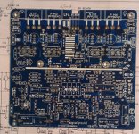
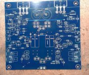
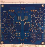
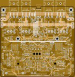
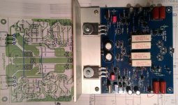
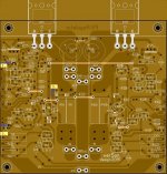
Attached some boards photos, first one with the soldering mask errors. I built first amp with that board and attached are photos of the amp in listening session. Only one board was assembled and listening impression is similar to that of the 200 W version, just in mono.
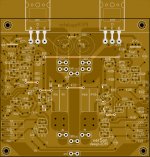
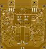
Other photos are of the amp board with no errors and PS regulator board.
Damir
Here is the previous list of order:
platon.rado-6 pieces/only power amp pcb/
Cambe- 2 Amp PCB's and 2 Reg PCB's.
Ajit- 2 Amp PCB's and 1 reg pcb
ejno - 2 amp PCB's and 2 Reg PCB's
vac231 - 2 amp PCB's and 2 Reg PCB'
Joshvi- 2 Amp PCB's and 1 reg pcb
I have now more pcbs to offer, 20 amp boards with no soldering mask errors for 19 EURO + shipping, more then 20 amp boards with the soldering mask errors(easy to rectifier by rub off some protective paint) for 13 EURO + shipping and 10 PS Regulator boards for 19 EURO + shipping.
Attached some boards photos, first one with the soldering mask errors. I built first amp with that board and attached are photos of the amp in listening session. Only one board was assembled and listening impression is similar to that of the 200 W version, just in mono.
Other photos are of the amp board with no errors and PS regulator board.
Damir
Attachments
-
 PCB-bottom-photo.jpg358.5 KB · Views: 1,100
 -
 amp assembled-2.jpg379.8 KB · Views: 1,056
 -
 100W CFA prvo ugadjanje.jpg294.3 KB · Views: 1,023
 -
 100W CFA prvo slusanje.jpg200.7 KB · Views: 997
 -
 amp top side.jpg244.9 KB · Views: 972
 -
 amp bottom side.jpg172.8 KB · Views: 448
 -
 PS-R-top-side.jpg234.2 KB · Views: 345
 -
 PS REgulator bottom side.jpg149.5 KB · Views: 352
I downloaded the post775 .zip
saved all three files to my ltspice folder.
When I "run", I get lots of warnings. The missing diodes I can correct for.
What do I do with the rest?
Most of diodes are from the LT library. There two txt files inside the zip file with models. It should be opened in the same directory where is .asc file.
I said I saved all three files to my lt spice folder. (note the duplicate devices warning, you have the same device called up more than once in one txt file.)
Any idea why the diodes are not being read from the lt spice library?
What about the other warnings?
Any idea why the diodes are not being read from the lt spice library?
What about the other warnings?
I said I saved all three files to my lt spice folder. (note the duplicate devices warning, you have the same device called up more than once in one txt file.)
Any idea why the diodes are not being read from the lt spice library?
What about the other warnings?
I don't know why some diodes not being read fro the LTspice library.
What other warnings in particular?
the warnings are shown in the attachment post904
Forget duplicate device warnings, not important, and I don't have other warning when I extract the files and run .asc.
100 W CFA assembling instruction
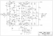
I would like to explain in a few words how to assemble this amp. First step is to solder IPS (input state) up to the VAS/TIS. That means looking the schematic from the left up to the VAS/TIS transistors (Q6/Q8) and the capacitance multipliers on both polarity (Q9, Q10). After connection the power supply (there is no big risk of high current in that stage) it is necessary to check the currents trough R5 and R6. It should be around 1.4 to 1.5 mA (easiest way to do that is to measure the votage drop on those resistors). This current is dependent of the CCS current, defined with LEDs D11, D12 and emitter resistors R4, R7. The Leds should be ordinary red type. If the current trough R5, R6 is to much out of range then can be changed by changing R4, R7 value, a bit up or down. Also is good to match the LEDs.
After that is possible to assemble the rest of the board minus the drivers (Q6, Q8). The current trough resistors R14, R52 should be between 4 and 8 mA (you see it is not to critical).
Before to solder the drivers in place set the trimmer P1 to the max value. After the drivers are soldered it is necessary to set the output transistor bias current. It should be between 130 to 150 mA. If you use the alu bracket as in my example you can do that with no main heat sink, but not for to long as output transistor temperature will rise slowly but steady.
The layout is a bit different from most used. Output transistor and corresponding electrolytic capacitor are in order looking from the left side of the PCB IRFP240, IRFP9240, IRFP240, IRFP9240. Don’t put any elco upside-down.
Whit no DC servo op-amp in socket output DV voltage will not exceed 100 mV, and with the op-amp in place that should be close to zero voltage.
I wish you good building.
I added the link to this post to the first post.
Damir
Attachments
PS regulator assembling and testing instruction
This PS regulator contains following protection: overcurrent protection, loudspeaker DC offset protection and protection against bigger then allowed differences in +- output voltage. If any protection was triggered both power supply polarity will switch off simultaneously. To switch on again it is necessary to switch off the mains power for few minutes to allow big caps to discharge.
All component can be assembled for first power on, minus switcher transistors Q7 and Q107. This is because minus output polarity should be set equal positive output polarity first. Put some load on both outputs
If there is output voltage on the out + and it should be 6 to 7 volts lower then in + then set to the same value out – with trimmer P1.
When that was set solder in transistors Q7 and Q107. Now is possible to test the PS regulator. With 0.11R for R9 and R109(This will limit to about 11 A, to lover it short one diode D3 and D103) the current sensing transistors Q6 or Q106 should trigger Q8, Q9 or Q108, Q109. Those transistors are in the configuration similar to thyristor and when triggered transistor Q7 or Q107 will conduct and switch of output serial transistor Q13, Q113.
The pins LL and LR are DC offset sensor inputs when connected to the power output. Connect there 10 V or more (to any input) and it will trigger the same “thyristors” with delay defined with RC constant of R18/C4, R19/C5 (similar on minus side) and switch off the outputs transistors.
One important feature is simulant switch off of both polarity because of differences in the output voltage recognized via zeners D6 and D7.
Damir
Attachments

Last edited:
How much power (Amps) you can draw safely from this PSU?
What size of heatsinks needed?
Depends of transformers used. PS regulator will provide up to 11 A.
100W CFA and PS Regulator board
To summarize orders and delivers for the 100W CFA anf PS regulator boards:
platon.rado...6 pieces/only power amp pcb/ ....shipped
Cambe...2 Amp PCB's and 2 Reg PCB's. .........shipped
Ajit...2 Amp PCB's and 1 reg pcb ..................no answer on PM
ejno... 2 amp PCB's and 2 Reg PCB's .............gave up
vac231... 2 amp PCB's and 2 Reg PCB's .........delivered
Joshvi...2 Amp PCB's and 1 reg pcb ...............shipped
dady..2 Amp PCB’s ......................................no answer on PM
If there are more interested, I have more boards left, Amp boards with no solder mask error(19EUR) and with error(13 EUR), PS Reg. boards(19 EUR) and I prefer to sell it together with amp boards.
Damir
I have to report another small layout error on the PS regulator board.
First one was C3 to be reversed, and second one is missing trace between wiper and left pin of the trimmer P1. It could be done simple by soldering wiper pin and left pin together, looking from the bottom side. Attached the picture.
Damir
First one was C3 to be reversed, and second one is missing trace between wiper and left pin of the trimmer P1. It could be done simple by soldering wiper pin and left pin together, looking from the bottom side. Attached the picture.
Damir
Attachments

In my Country we say, third time for luck.
Here is third PS regulator layout error. Zener D6 should be reversed, the layout below.
1. P1 pins to be shorted.
2. C3 to be reversed.
3. D6 to be reversed.
My sincere apology even if all of the errors are easy to rectify, no need to change the layout.
Damir
Here is third PS regulator layout error. Zener D6 should be reversed, the layout below.
1. P1 pins to be shorted.
2. C3 to be reversed.
3. D6 to be reversed.
My sincere apology even if all of the errors are easy to rectify, no need to change the layout.
Damir
Attachments
Last edited:
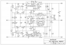
This is PS regulator with MOSFET output transistor. It works similar as the one with BJT output but can provide higher current before the current sensing go on. Maximal current per rail is 20 A and can be set to 17 A if one diode in the current sensor was bridged.
If anyone interested in a PCB, please, let me kow.
Damir
If anyone interested in a PCB, please, let me kow.
Damir
Attachments
- Home
- Amplifiers
- Solid State
- 200W MOSFET CFA amp