Dadod
Have you put a schematic up that has the expected voltages on it for the front end? Thanks
Chris, it is here.
Damir
Attachments
Chris, it is here.
Damir
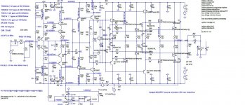
There is one thing that puzzles me about this diagram.
F.ex. on the positive side, the GS voltage protection zeners D6 & D3 are connected to the emitter followers Q5 & Q9
I think that if the output is shorted to ground with signal on the input, the lack of feedback signal will force Q6 to conduct fully and draw the EF's to the rail, destroying either/both the EF's and/or zeners and also smoking the output devices when the zeners/diodes burns to open circuit.
The same happens on the negative side too.
Do you have any comments on this?
And is there any analyzes made of the consequences when the zener protection diodes comes into conducting?
Normally the VGS protection zener diodes are connected to the VAS outputs (Q6 & Q8) collectors and provisions should be made to limit the max current.
JohanB
To be honest I never thought to much about this protection, just that it should protect the mosfet gates from excess voltage.
I simulated now with protection zeners connected to the VAS outputs and it looks you are right to some degree. The zeners will not be destroyed but still output current will be to high for the output mosfet.
Another advantage, I spare one set of the protection diodes in this amp.
Anyhow I am going to use my PS regulator incorporated with all needed protection for this amp.
Damir
...
I think that if the output is shorted to ground with signal on the input, the lack of feedback signal will force Q6 to conduct fully and draw the EF's to the rail, destroying either/both the EF's and/or zeners and also smoking the output devices when the zeners/diodes burns to open circuit.
The same happens on the negative side too.
...
If Q6 would conduct fully, Q5 and the output mosfets even would conduct fully which is equivalent to shorted positive rail voltage ...
One MOSFETs can withstand a pulse drain current of 80A x 4 = 320A
With some of luck only the power supply fuse will die ...
To be honest I never thought to much about this protection, just that it should protect the mosfet gates from excess voltage.
I simulated now with protection zeners connected to the VAS outputs and it looks you are right to some degree. The zeners will not be destroyed but still output current will be to high for the output mosfet.
Another advantage, I spare one set of the protection diodes in this amp.
Anyhow I am going to use my PS regulator incorporated with all needed protection for this amp.
Damir
Yes, but protection in the power supply can not protect individual smaller components that are overloaded and go up in smoke in milli-Seconds.
I see you have changed the value of R20 & R24 first from 220R to 6K8 and now to 15K0 and R16 & R29 from originally 680R to 470R, which results in a maximum possible -2Volt on the base of Q6 referred to the rail.
This restricts the peak current through Q6 to around 20mA (R34,C4 not accounted as they only works at higher frequencies), which is within the SOA limits for the C3503/A1381, so the zeners/4148's will also survive and everything seems to work that way.
Maybe the zener diode voltage can then be of a little lower value.
10-12Volt will probably do fine, to also limit the MOS-FET's peak current, before your power supply protection or fuses cuts in.
Johan
Hi Johan,
Thank you for your help. I can see that you have followed this thread if you noticed those resistor changes.
Simulation shows 200 mA of the peak current through Q6, but I see how you calculated 20 mA. Why simulation is so much over?
My PS regulator has a kind of electronic fuse with progressively decreasing acting time when the current increases and it's quite fast.
Damir
Hi Damir,
I also like to thank you for doing this comprehensive research about CFA amps.
I'm quite impressed by the very low distortion figures you published.
But I'm a little confused about the extensive frequency compensation networks in your application.
Are these only products of simulations or do they work in real life?
Must be highly dependent of circuitry layout at these frequencies!
How did you do these calculations?
Johan
Hi Johan,
This is real amp, my first prototype is here http://www.diyaudio.com/forums/solid-state/243481-200w-mosfet-cfa-amp-74.html#post4278243.
RNMarsh has this one and he did some measurements and listening, the results are somewhere in this thread. Astx made his first board, some post back are some results.
This compensation is actually two compensation in parallel plus some help from RC combo at the VASs emitters. First compensation is TPC(C7, R1, C6 and C14, R1, C9) and second some kind of Cherry two poles compensation(C8, R1, C6 and C8, R1, C9).
BR Damir
This restricts the peak current through Q6 to around 20mA (R34,C4 not accounted as they only works at higher frequencies), which is within the SOA limits for the C3503/A1381, so the zeners/4148's will also survive and everything seems to work that way.
There s another non limited current path..
As pointed for another such design this path through Q6 is limited by a 130R total resistance, from ground through R22 and R46, then through Q3/Q33 collector/emitters and then through the base/emitter junction of Q14/Q6 and this latter s 100R degeneration resistance.
The cure is a few Kilohom resistance in serial with Q33/Q34 collectors, as can be seen in many old designs.
I've never seen any of your design old or new(?) but I suppose in series with Q33/Q34 emitters?
P.S.
OK, I see now it can be in series with collectors.
Last edited:
I've never seen any of your design old or new(?) but I suppose in series with Q33/Q34 emitters?
P.S.
OK, I see now it can be in series with collectors.
I said in the collectors, and my designs have nothing to do with this point, set apart that i implemented this component when i build a basic CFA when i was 14 year old, it was the main flaw in Motorola s application note describing this amp IIRC.
Last edited:
I said in the collectors, and my designs have nothing to do with this point, set apart that i implemented this component when i build a basic CFA when i was 14 year old, it was the main flaw in Motorola s application note describing this amp IIRC.
I new you are genius, I made my crystal detector when I was 10.
I new you are genius, I made my crystal detector when I was 10.
I was talking of CFAs and about a basic feature that need no genius but a few neurones, that s not all to shoot for some perfs , the first quality of a design is reliability and ease of build.
I was talking of CFAs and about a basic feature that need no genius but a few neurones, that s not all to shoot for some perfs , the first quality of a design is reliability and ease of build.
I don't agree that a few neurons are enough, I did not come to that solution.
Reliability yes, easy to build no.
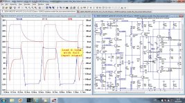
I think that now this amp has quite good protected against output short connection.
This plot shows the VAS and zener current with 0.1 ohm at the output and full signal at the input. Max MOSFET current is a bit more then 36 A.
I would like to thank all who came with suggestion how to do that.
Damir
This plot shows the VAS and zener current with 0.1 ohm at the output and full signal at the input. Max MOSFET current is a bit more then 36 A.
I would like to thank all who came with suggestion how to do that.
Damir
Attachments
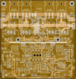
Hi Dadod
You could not give gerber files 200W MOSFET???
Thanks
No, sorry. I will offer some PCBs, be patient.
This is 100W/8ohm, 200W/4ohm version of the same amp. I think this power is very well suited for use in active loudspeakers, and of course for stand alone amplifier too.
I am ready to offer the PCB for this amp if there is going to be enough interested people, so let me know.
I am ready to offer the PCB for this amp if there is going to be enough interested people, so let me know.
Attachments
- Home
- Amplifiers
- Solid State
- 200W MOSFET CFA amp