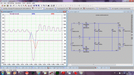
Did your sim model have any real L and series r (R of transformer winding, esr, diode drop vs current etc)? And, did you measure the delta or differentially (across the V+ to V-)?
There must be some real drop in voltage if you loaded one side more than the other. Thus a delta, too.
[PS - years ago, I had an engineer at LLNL do a sim in SPICE and it worked fine for him/me. Brian Elliot - HP and IBM researcher, got it when explained to him. I suspect your sim isn't realistic enough or measured at wrong places.]
Thx-RNMarsh
Last edited:
Did your sim model have any real L and series r (R of transformer winding, esr, diode drop vs current etc)? And, did you measure the delta or differentially (across the V+ to V-)?
There must be some real drop in voltage if you loaded one side more than the other. Thus a delta, too.
[PS - years ago, I had an engineer at LLNL do a sim in SPICE and it worked fine for him/me. Brian Elliot - HP and IBM researcher, got it when explained to him. I suspect your sim isn't realistic enough or measured at wrong places.]
Thx-RNMarsh
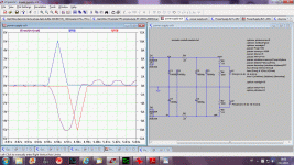
This is with 100 Hz 10 A current pulses. As you can see, I don't have transformer but instead 2 ohm resistors to simulate the transformer loses.
BR Damir
Attachments
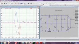
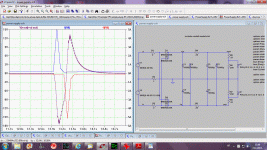

All my technical knowledge was telling me that the across connected cap should only worsened the tracking. If I used ten times bigger capacity for across connected then the caps connected between + and – polarity and the ground then tracking effect should be more pronounced, isn’t it? I simulated two cases, first normally connected caps with the values 1000 uF + 10000 uF connected between + and – polarity and the ground, and then second with 1000 uF connected normally between + and – polarity and the ground, and 10000 uF across connected cap. Then I simulated with with constant current of 360 mA between polarities and then 10 A 100 Hz current pulses between polarities and the ground mimicking an AB class amp.
Here is result and it shocked me as I did not expected that terrible behavior with the across connected cap!!
Am I wrong here? I did not use a transformer as there is no model in LTspice and I did not add any inductance, I think it will not change essence of this simulation.
BR Damir
Here is result and it shocked me as I did not expected that terrible behavior with the across connected cap!!
Am I wrong here? I did not use a transformer as there is no model in LTspice and I did not add any inductance, I think it will not change essence of this simulation.
BR Damir
Attachments

............
I would like to suggest something:
1. Insert input polypropylene cap in the input, 1 uF is high enough value.
2. Insert a trim pot of 200 ohm parallel to the R15, R23, then change those resistors from 15 ohm to 18 ohm, this to trim output DC offset.
3. Q5 and Q6 should be for higher voltage as almost all power supply voltage is on them.
4. Q11 and Q16 should have own smal heath sinks as thy dissipate 1.7 W max.
5. Q17, Q20, Q22 and Q23 should also have own small heath sinks, max dissipation 1.2 W.
6. Electrolytic caps for the OPS don’t need to be of so high value, max 1000 uF is more then enough.
7. Resistors R51 and R52 use 33 ohm instead 82 ohm.
8. Put one jumper between R42 and R46 midle point and feedback input point, in this way one can decide to use high or low feedback and decide by listening the preference.
9. R88(R9 in my schematic) should be of 1 W.
BR Damir Verson
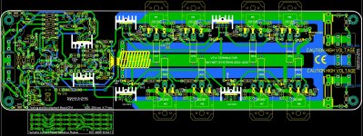
Dadod, I've modified the schematic/layout per your suggestions and here is the update.
I wasn't able to find the ready-made heat sinks that will work with the tight layout so I decided to rig a 125 mm long aluminum plate and mount all 6 TO-126 on it. The aluminum plate is to be affixed on the PCB at two mounting holes.
Trim pots are now SMT too. They are Bourns 3224G side adjust type. Both are placed towards the top edge of the PCB. Bias pot is on the top side, and the DC offset pot is on the bottom side. Perhaps the offset pot is a bit hard to spot in the picture. Look for the three pads in purple color between Q2 and Q3.
Attachments
Dadod, I've modified the schematic/layout per your suggestions and here is the update.
I wasn't able to find the ready-made heat sinks that will work with the tight layout so I decided to rig a 125 mm long aluminum plate and mount all 6 TO-126 on it. The aluminum plate is to be affixed on the PCB at two mounting holes.
Trim pots are now SMT too. They are Bourns 3224G side adjust type. Both are placed towards the top edge of the PCB. Bias pot is on the top side, and the DC offset pot is on the bottom side. Perhaps the offset pot is a bit hard to spot in the picture. Look for the three pads in purple color between Q2 and Q3.
Very nice! Is this final or you have to do something more?
On first glance I noticed different value for some resistors. You correctly chose higher wattage for resistor parallel to the inductor but it should be of 1 ohm, and R57 to be of 6.8 ohm 2W.
I simulated a high frequency local Zobel network per individual MOSFET and it did not make any harm nor improvement.
Did you use multiturn trim pot?
What kind of small caps(compensation and in RC for mosfets) did you use? Ceramic NP0 or C0G are OK for that.
I would need more time to check other things as is so tightly packed.
Thanks a lot
Damir
Last edited:
Very nice! Is this final or you have to do something more?
On first glance I noticed different value for some resistors. You correctly chose higher wattage for resistor parallel to the inductor but it should be of 1 ohm, and R57 to be of 6.8 ohm 2W.
Did you use multiturn trim pot?
What kind of small caps(compensation and in RC for mosfets) did you use? Ceramic NP0 or C0G are OK for that.
I would need more time to check other things as is so tightly packed.
Thanks a lot
Damir
It is close to final but I'm open to ideas. I am also going to put the empty upper right corner to some use. Perhaps a connector that takes 10VAC, a bridge rectifier, for the solid state relay and a power-on delay circuit.
The trim pots are multi-turn type.
All SMT caps except the 0.1uF are C0G 500v or 1kv.
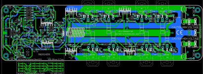
Some progress on the board. Okay for comments... so fire away. This is just for input, it is NOT finished, but hopefully soon.
This is very nice too! So we are going to have a choice, all trough the hole PCB and PCB combining both SMT and trough the hole devices. This PCB from nattawa includes a loudspeaker protection with solid state switch.
I suggested to use my regulated tracking full protection power supply and in this case solid state loudspeaker protection is not needed and could be omitted from the PCB, but now we need someone to design regulated power supply layout.
BR Damir
dadod,
How do you cancel differential-mode noise on a pair of wires? And how would you measure it? Just something to ponder in the background. Tracking regulators take care of the Differentail-Mode issue. But there are passive ways as well. Enough said.
Looks like a great Current-feedback amp and am looking forward to the test results when built. It has the power output that I would require for my home system.
-RNM
Last edited:
dadod,
How do you cancel differential-mode noise on a pair of wires? And how would you measure it? Just something to ponder in the background. Tracking regulators take care of the Differentail-Mode issue. But there are passive ways as well. Enough said.
Looks like a great Current-feedback amp and am looking forward to the test results when built. It has the power output that I would require for my home system.
-RNM
Richard you like riddles, I am not good at it. You should know that I am telecommunication engineer, retired software specialist, audio and electronic is just my hobby so you could be more specific.
You did not comment my simulations about passive tracking, was it good enough??
BR Damir
Richard you like riddles, I am not good at it. You should know that I am telecommunication engineer, retired software specialist, audio and electronic is just my hobby so you could be more specific.
You did not comment my simulations about passive tracking, was it good enough??
BR Damir
It wasn't for you alone, but for anyone reading this. Someone else might comment. Doesn't matter, you got the tracking volt regulator idea to use. I had some questions about the sim. But don't need to go into it here... it would be a whole other subject. Let me leave it at this --- how do you cancel differential signals on the + and - ps lines? That is, the signals on the power supply wires which are out of phase. A cap between them will cause them to cancel. From there we can go further.... but. not here. Sorry don't have the time right now. When I do, I'll do both sim and actual measurements for everyone.
Thx-RNMarsh
It looks like nobody wants to comment?
After I did that previous simulation I came to conclusion that across connected capacitor should be of lower value that the main capacitors, let say ten times lower. If the main cap is 10000 Uf than across connected cap could be 1000 uF paralleled with quality film cap(polypropylene) of 10 uF(to cancel high frequency differential signals).
BR Damir
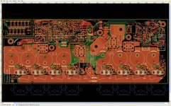
The OPS is ready for check.
Chris here are my suggestion for the moment:
1. R36 should be of 2 W
2. Change Q17 to 2SA970 and Q19 to 2SC2240
3. Put Q3 closer to Q4 to shorten between connections.
4. Move the front end power supply connection to the right between the front end and the OPS
5. Add possibility to power the front end from the same power supply as it is in the schematic, adding 33 ohm reistors and 1000 uF caps. Connect the front end power ground to the OPS power ground.
6. Add 10 ohm resistor between the frond end power ground and the front end signal ground.
7. It could be nice to use power resitor Caddock MP915 470 ohm 1% for R37, DigiKey has it.
http://www.caddock.com/Online_catalog/Mrktg_Lit/MP9000_Series.pdf
BR Damir
Attachments

It looks like nobody wants to comment?
After I did that previous simulation I came to conclusion that across connected capacitor should be of lower value that the main capacitors, let say ten times lower. If the main cap is 10000 Uf than across connected cap could be 1000 uF paralleled with quality film cap(polypropylene) of 10 uF(to cancel high frequency differential signals).
BR Damir
Yes to all... a few too many zero's. Even on +/- 15vdc regulated circuits, I use about 100mfd (105C) bypassed with at least .22mfd film. Could be larger. But on an unregulated supply larger values ("up to" the main supply values) are beneficial. Easy to try a bridging cap values and then listening. There are some measurements which show improvements as well. Your suggestion of bridging with 1/10 value is a good one to use. Enjoy!
Thx-RNMarsh
Last edited:
Any more comments and or corrections before I start on Ver 3.0?
Dadod are you saying that the separate front power is out, or is that an option?
Dadod are you saying that the separate front power is out, or is that an option?
Any more comments and or corrections before I start on Ver 3.0?
Dadod are you saying that the separate front power is out, or is that an option?
I would say an option, make provision with faston connector for separate front end power supply and add 33 ohm resistors and 1000 uF caps. I think that you used to small footprint for 1 uF input cap.
BR Damir
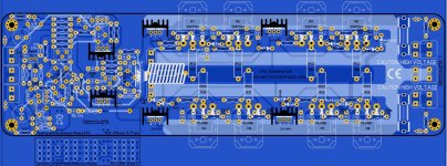
This is my final SMT CFA layout. Hopefully the new color scheme renders a better visibility for reviewers. Nothing has been changed except for the added optional supply and delay circuit to the solid state speaker relay control and some touch up work to the details. Dadod, if you'd like Gerber files for an in depth review please send me a PM.
I think I'll be able to find some time to layout your regulated PSU design next month, Dadod, if no one else has picked it up by that time.
I think I'll be able to find some time to layout your regulated PSU design next month, Dadod, if no one else has picked it up by that time.
Attachments
Looks good guys,
Not sure if you want to lower the input R less than 47K to reduce noise, if so, might want to use consider these parts
505-MKS210/50/20
10uF/50V 16x11 LS 5mm 0.5 lead
Another option is
667-ECQ-V1H225JL
2.2uF/50V 10.2x8 LS 7.5mm
Not sure if you want to lower the input R less than 47K to reduce noise, if so, might want to use consider these parts
505-MKS210/50/20
10uF/50V 16x11 LS 5mm 0.5 lead
Another option is
667-ECQ-V1H225JL
2.2uF/50V 10.2x8 LS 7.5mm
- Home
- Amplifiers
- Solid State
- 200W MOSFET CFA amp