...but this device is looking promising:
http://datasheets.maxim-ic.com/en/ds/MAX15012-MAX15013B.pdf
(May be a an additional PNP for fast gate pull down)
http://datasheets.maxim-ic.com/en/ds/MAX15012-MAX15013B.pdf
(May be a an additional PNP for fast gate pull down)
...the spec looks nice, but just at first glance.
There is a minimum pulswidth requirement and the Maxim proposal to overcome this is OK for SMPS, but not classD IMHO.
To use this IC properly in class D we would need a duty cycle limitation at the comparator input... Ugly.
There is a minimum pulswidth requirement and the Maxim proposal to overcome this is OK for SMPS, but not classD IMHO.
To use this IC properly in class D we would need a duty cycle limitation at the comparator input... Ugly.
It's not that bad, short pulse widths are only required either when the output is very close to the rails or when the rate of change of output voltage is close to the slew rate limit imposed by the output filter. In both cases you will already have distortion.
I started to play with a triangle modulator followed by a fast level shifter.
The comparator was the LT1711 and the isolator/level shifter a HCPL9030.
The HCPL is known as fast, but critical with.
AD has made a comparison and is stating that with noise you might cause the HCPL to go for wrong HIGH signal at the output.
http://www.analog.com/UploadedFiles/Product_Highlights/5406830898840Agilent_NVE_FMR_IsolatorsF.pdf
Up to now I was not able to force this misbehavior. HCPL9030 acts like a nice guy so far in my breadboard set up.
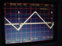
More difficult seems to be to settle a blameless triangle modulator for pulses below 10ns. In myexperiment the pulses are becoming instable and jittering below 10ns.
Please note that my screen shots show the triangle and the output of the HCPL, the output pulse of the LT1711 happens a few ns earlier,
First screen shot unzoomed with 50ns/Grid.
Triangle is shown with 100mV/Grid
Output of the HCPL with 2V/Grid
The comparator was the LT1711 and the isolator/level shifter a HCPL9030.
The HCPL is known as fast, but critical with.
AD has made a comparison and is stating that with noise you might cause the HCPL to go for wrong HIGH signal at the output.
http://www.analog.com/UploadedFiles/Product_Highlights/5406830898840Agilent_NVE_FMR_IsolatorsF.pdf
Up to now I was not able to force this misbehavior. HCPL9030 acts like a nice guy so far in my breadboard set up.
More difficult seems to be to settle a blameless triangle modulator for pulses below 10ns. In myexperiment the pulses are becoming instable and jittering below 10ns.
Please note that my screen shots show the triangle and the output of the HCPL, the output pulse of the LT1711 happens a few ns earlier,
First screen shot unzoomed with 50ns/Grid.
Triangle is shown with 100mV/Grid
Output of the HCPL with 2V/Grid
Attachments

In fact I am not convinced that it is really necessary to squeeze down the last few ns of delay.
With a IRS20955+NPN/PNP-driver I can go for roughly 200ns delay between comparator input and halfbridge output.
If I spend a lot of efforts with a HCPL level shifter and additional drivers - and have to settle all shut down functions in discrete... then I could reduce this to roughly 120ns.
...so now compare this to the group delay of the output filter of an class D amp. The typical step response is 10us-20us delayed to the input signal...
Is it really worth to squeeze the overall delay from 15us down to 14.92us and run into a complex circuit with high component count? 🙄
....but I start to like this more & more:
http://focus.ti.com/docs/prod/folders/print/ucc27200.html
Thanks to Lumanauw for inspiration. 🙂
http://focus.ti.com/docs/prod/folders/print/ucc27200.html
Thanks to Lumanauw for inspiration. 🙂
...and with respect to the fact that my topology has a di/dt limiter I might even dare to use this...
http://www.maxim-ic.com/quick_view2.cfm/qv_pk/5016
http://www.maxim-ic.com/quick_view2.cfm/qv_pk/5016
Hi, Choco,
Beware that they are very hot small chip 😀 And be carefull in the experiment, they are fragile, not so tolerant like discrete designs. Better buy the DDA version (thermal pad), and design the PCB so the groundplane is also used for heatsinking this tiny hot chip. I buy all SOIC, now I have to re-buy the DDA version.
They are about the same with LM5100/5101 and HIP2100/2101
...yes I know. With my MosFets I will theoretically end up
with 500...600mW driver losses at 350kHz, which is already quite a lot for such a small casing. Probably an external PNP for gate pull down would be a reasonable countermeasure.
Speeding up the turn off and moving some losses out the IC towards external BJTs.
with 500...600mW driver losses at 350kHz, which is already quite a lot for such a small casing. Probably an external PNP for gate pull down would be a reasonable countermeasure.
Speeding up the turn off and moving some losses out the IC towards external BJTs.
From the datasheet note, one thing can be done to lessen the heat of the chip. To put external bootstrapp dioda. This dioda contributes to significant heat of the whole chip. But this external dioda has to be ultrafast with Vf<0V65.
...yupp, if supplying the high side by bootstrapping - I think that is helpful.
But I am planning to stick to my solution with a floating flyback supply for the High Side, like in my proto.
I started to love the fully reliable high side driver supply at all load conditions no matter if clipping or not.
And it completely avoids losses in the boot strap diode.
But I am planning to stick to my solution with a floating flyback supply for the High Side, like in my proto.
I started to love the fully reliable high side driver supply at all load conditions no matter if clipping or not.
And it completely avoids losses in the boot strap diode.
Good then 😀
I look at the graph, the dioda dissipation is about 1/2 of the total heat dissipation. That is big. But what dioda can be used? MUR140 or 1N4148 has VF about 0V65. Schottky is the one that has lower drop, but we need high reverse voltage as well.
I look at the graph, the dioda dissipation is about 1/2 of the total heat dissipation. That is big. But what dioda can be used? MUR140 or 1N4148 has VF about 0V65. Schottky is the one that has lower drop, but we need high reverse voltage as well.
Choco,
Why I seldom see so low inductance output filter (+big capacitance) like you use (5uH)? You've given your reasons before, what are the drawbacks of this approach?
Why I seldom see so low inductance output filter (+big capacitance) like you use (5uH)? You've given your reasons before, what are the drawbacks of this approach?
- Status
- Not open for further replies.
- Home
- Amplifiers
- Class D
- 1kW Gen2