
post58
Q6 emitter loading is very different from the emitter loading of 5.
Will this make much difference to the performance of the amplifier?
Yup, it could be corrected by connecting a 100~220 ohm resistor to the emitter of Q6. It wont make any difference in performance of the amp, but will change bias. so, bias needs to be readjusted.
I have connected a jumper on the emitter of Q6 in the PCB, to insert this resistor, if you need to.
Yes, you can replace but you have to use several pairs of TIP41C / TIP42C (at least 8 pairs 41C/42C on 2 ohm impedance and with power supply as I said in post no.24).thanks my friend
can i replace mje15034, mje15035 with tip41c and tip42c ?
Q3 transistor (BD139) is not protected. Without emitter resistance (eg. 22 ... 100ohm) that transistor will don't have a long life. Besides that resistor you need another transistor and another resistor. If you connect that resistor will see that THD will increase and performance will get worse.schematic attached.
So, your schematic amplifier work very well theoretical but practically will not be reliable.
Last edited:
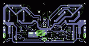
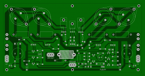
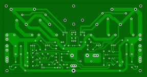
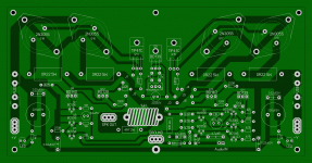
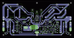
proposed PCB, parts marking needs to be done.🙂
can you please share silk screen and botome side in PDF file ?
i want use iron and laser jet printer for creat pcb.
silk screen need parts value too.
thanks
Yup, it could be corrected by connecting a 100~220 ohm resistor to the emitter of Q6. It wont make any difference in performance of the amp, but will change bias. so, bias needs to be readjusted.
I have connected a jumper on the emitter of Q6 in the PCB, to insert this resistor, if you need to.
what is this mean ?!
show me in your PCB please
thanks for your helping dear
Q3 transistor (BD139) is not protected. Without emitter resistance (eg. 22 ... 100ohm) that transistor will don't have a long life. Besides that resistor you need another transistor and another resistor. If you connect that resistor will see that THD will increase and performance will get worse.
So, your schematic amplifier work very well theoretical but practically will not be reliable.
Hi Donpetru,
Q3 transistor is not protected from what?? please elaborate.
Q3 is the VAS transistor and is beta enhanced by Q14, VAS current is 8mA, it won't see anything greater than 30V across CE for +/-30V supply voltage. I agree with you with resistor connected THD will increase, to my personal experience without this resistor Bass is tighter. but to aid reliability a 10 ohm resistor would be connected in the final schematic.
If you see closely i have already connected a resistor to Q3 emitter on the PCB which can be replaced with a jumper if you want.
what is this mean ?!
show me in your PCB please
thanks for your helping dear
Hi Hadighorbani,
give me some time pal, would post the final schematic and PCB files soon.
I would also want to say clearly, that Multisim is a great simulation software, easy to use, conservative, has almost all spice models. above all, the simulation results are very much close to the practical working circuit.
I have simulated my 3 working designs in Multisim and there are just minor differences in the simulation and actual working circuit. I trust this software and it won't let us down.
Cheers!!!!🙂
Aniket
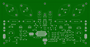
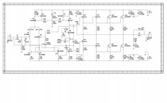
Final schematic and gerber files attached.
Regards,
Aniket🙂
Regards,
Aniket🙂
Attachments
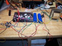
Circuit of Post #26, working perfectly. Finally got to a test with actual speakers. At the low voltage and current levels in the front end, I would recommend small signal transistors in the VAS and predriver, not the BD139's.
Biased at 10mA per output and it appears to be plenty. That one channel is pretty darn loud driving two dual driver PA cabs.
Biased at 10mA per output and it appears to be plenty. That one channel is pretty darn loud driving two dual driver PA cabs.
Attachments
proposed PCB, parts marking needs to be done.🙂
Hi Aniket, your layout design is very well. Which software are you using?
Regards.
Circuit of Post #26, working perfectly. Finally got to a test with actual speakers. At the low voltage and current levels in the front end, I would recommend small signal transistors in the VAS and predriver, not the BD139's.
Biased at 10mA per output and it appears to be plenty. That one channel is pretty darn loud driving two dual driver PA cabs.
That's great wg_ski,
Hadighorbani you have 1 working amp ready.🙂
Since, the final load would be 2 ohm, predriver and VAS would be under stress, so i have used BD139/40, BD's are more robust than small signal one's, and they sound pleasing also.
Hi Aniket, your layout design is very well. Which software are you using?
Regards.
Hi terranigma,
I use Sprint Layout 6.
Regards,
Aniket
Look at the picture below. Transistor Q20 is very important to protect the VAS transistor Q3. That transistor will increase the THD value of the amplifier but not very much.Hi Donpetru,
Q3 transistor is not protected from what?? please elaborate.
Aniket
Attachments
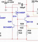

I concur that some protection for the VAS transistor is a good idea. This is because you chose, and wisely, to use a beta-enhanced VAS. This configuration can deliver a lot of current to the VAS base and overdrive it. An alternative is to use some resistance in the collector of the beta-enhancer transistor to limit the available drive to the VAS, though not as effective as adding a transistor and some emitter degeneration to shunt drive current away on an overload situation.
In 'normal' operation it isn't likely to be an issue, but if driven into hard clipping or a short / low impedance at the output (or a transistor failure for that matter) the VAS will be at risk.
In 'normal' operation it isn't likely to be an issue, but if driven into hard clipping or a short / low impedance at the output (or a transistor failure for that matter) the VAS will be at risk.
Final schematic and gerber files attached.
Regards,
Aniket🙂
Is the drill data missing from the Gerber?
Try this.hi every body
i have some 2n3055 with to3 case
i want creat amp with that for 120watt power in 2 ohm loud
please help me to fin this amp
thanks
Attachments
Try this.
A single pair 2N3055 @ 30V won't survive 2 ohm load for long.
Isn't that upper triple one of those configurations that oscillates like crazy? Especially if you go trying to parallel outputs to handle that 2 ohms.
- Status
- Not open for further replies.
- Home
- Amplifiers
- Solid State
- 120 watt amp in 2 ohm loud with 2n3055