After detailed check  ,of traces I find ,only one mistake as usual .
Corrected layout attached below , I will test as soon as I have some time to do this. I will report my results 😉
Regards ,Alex
,of traces I find ,only one mistake as usual .Corrected layout attached below , I will test as soon as I have some time to do this. I will report my results 😉
Regards ,Alex
Attachments
Last edited:
Please share the pdf with us Alex🙂After detailed check
Corrected layout attached below , I will test as soon as I have some time to do this. I will report my results 😉
Regards ,Alex
After detailed check
Corrected layout attached below , I will test as soon as I have some time to do this. I will report my results 😉
Regards ,Alex
Very nice to see the evolution of an amplifier 🙂!
Much fun, but a lot of work and time...
Great Job Alex!
regards Olaf
Attachments
Very nice to see the evolution of an amplifier 🙂!
Much fun, but a lot of work and time...
Great Job Alex!
regards Olaf
Agree,nice work as usual 😎 (german precision)
Regards,Alex
😀Agree,nice work as usual 😎 (german precision)
Regards,Alex
Now it must be only without error ...
regards Olaf
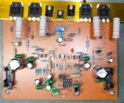
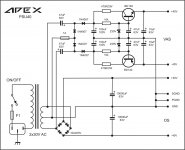
sorry, i wasn't thinking about that part of pcb: on the right it is "protect indicator" added from APEX-Zack NE555 protection and on the left there is clip indicator. that is added to a pcb but that does not affect the basic schematic of an amplifier or the way it works. i have had a free space on a pcb so that was the best way to use it,at the moment.
Did you make any changes to the layout? I am having issues on the negative rail on both boards.
Thanks, Terry
Did you make any changes to the layout? I am having issues on the negative rail on both boards.
Thanks, Terry
Can you post pictures?
Please share the pdf with us Alex🙂
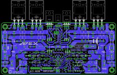
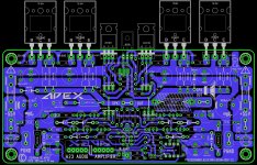
Files for PCB of A23 audio amplifier in .pdf format for toner transfer attached....🙂
Regards ,Alex
Attachments
Thanks Mr. pcb doctor🙂Files for PCB of A23 audio amplifier in .pdf format for toner transfer attached....🙂
Regards ,Alex
Did you make any changes to the layout? I am having issues on the negative rail on both boards.
Thanks, Terry
both versions work,one was done by me (with dual op-amp) and the other one by Djera (with single op-amp).
the latest files were only a little bit differente than Djera´s and my and all the difference is in a way of connecting GND from power supply to an amplifier PCB.
my and Djera´s pcb´s (first versions) have only main GND wire that goes from amp-pcb to a ground star of PSU,and newer pcb has PGND that should go with thicker wire to a PSU star GND,and two SGND that can be connected with not so thick wire,again to a star ground of PSU.
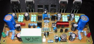
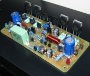
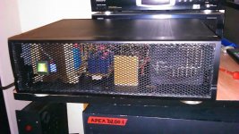
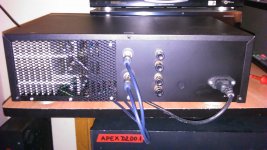
both versions should work fine,i just finished dual op-amp version,painted inclosure and wired completly:
Attachments
PCB correction
Sorry ,found another error ,I hope the last one 🙁 It's corrected ......🙂
So new files attached .... Files like : bottom and silk screen printed on transparent film foil can be used in photographic method as well if mirrored.
Regards Alex
Sorry ,found another error ,I hope the last one 🙁 It's corrected ......🙂
So new files attached .... Files like : bottom and silk screen printed on transparent film foil can be used in photographic method as well if mirrored.
Regards Alex
Attachments
Last edited:
both versions work,one was done by me (with dual op-amp) and the other one by Djera (with single op-amp).
the latest files were only a little bit differente than Djera´s and my and all the difference is in a way of connecting GND from power supply to an amplifier PCB.
my and Djera´s pcb´s (first versions) have only main GND wire that goes from amp-pcb to a ground star of PSU,and newer pcb has PGND that should go with thicker wire to a PSU star GND,and two SGND that can be connected with not so thick wire,again to a star ground of PSU.
both versions should work fine,i just finished dual op-amp version,painted inclosure and wired completly:
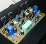
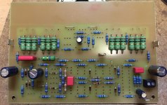
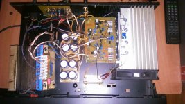
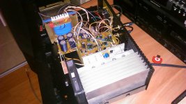
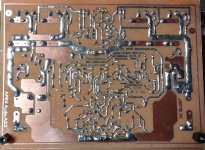
Here are some pics of one of my boards. Please look to see if you can find any errors. The board will not power up properly. I installed a 500R trimmer since the schematic shows 220R in that position. I didn't have 2W 1R so I installed 5W 0R33 emitters and I used two 1W 6K8 resistors in paralell for the 2W 3k3 resistors.
Thanks, Terry
Attachments
Pcb file
nice layout.. thanks for sharing ...
Regard
Files for PCB of A23 audio amplifier in .pdf format for toner transfer attached....🙂
Regards ,Alex
nice layout.. thanks for sharing ...
Regard
Here are some pics of one of my boards. Please look to see if you can find any errors. The board will not power up properly. I installed a 500R trimmer since the schematic shows 220R in that position. I didn't have 2W 1R so I installed 5W 0R33 emitters and I used two 1W 6K8 resistors in paralell for the 2W 3k3 resistors.
Thanks, Terry
changes you made are not a reason for problems you have. what op-amp do you use? re-check if there is any unwanted connections and if all the transistors are on their places,tourned as they should be. what to92 transistors do you use?
changes you made are not a reason for problems you have. what op-amp do you use? re-check if there is any unwanted connections and if all the transistors are on their places,tourned as they should be. what to92 transistors do you use?
I will have to go back and read though again. I used screenprint from post 3576. I see now that there are new versions. I used TL072. All TO92 are what are called out in the screen print. Without a matching schematic, trouble shooting is very difficult.
Thanks, Terry
I will have to go back and read though again. I used screenprint from post 3576. I see now that there are new versions. I used TL072. All TO92 are what are called out in the screen print. Without a matching schematic, trouble shooting is very difficult.
Thanks, Terry
Can you post voltage measurements on IC and transistors pins?
- Home
- Amplifiers
- Solid State
- 100W Ultimate Fidelity Amplifier